Assembly & Rework Microscopes
The production of electronics, automotive, medical devices and small mechanical parts often requires microscopy solutions for assembly and rework. Because it enables precise inspection and defect detection, microscopy helps meet strict industry standards and supports high-performance production in complex manufacturing processes.
Leica assembly microscopes come equipped with FusionOptics, a patented technology allowing you to see more detail in 3D while staying in focus at the same time. They also offer ergonomics for comfortable working conditions, and options to tailor the microscope to your sample and production environment needs.
Contact a local imaging specialist for expert advice on assembly and rework microscopes for your needs and budget.

How can quality be improved in assembly and rework?
Precise alignment of microscopic components during production, for both assembly and PCB rework, requires high-resolution visualization and magnification. Leica microscopes support accurate component placement and convenient manipulation under the microscope, thereby minimizing errors and improving overall quality.

How can productivity be enhanced on assembly lines?
Increasing productivity on the assembly line means sustaining higher levels of performance. Equipment designed to improve focus and reduce operator fatigue can help to enable this performance shift. Leica solutions, through Fusion Optics, enhance productivity through ergonomics for a comfortable working position and advanced optics that result in fewer microscope adjustments for the user.

How can the inspection of solder joints in electronics be improved?
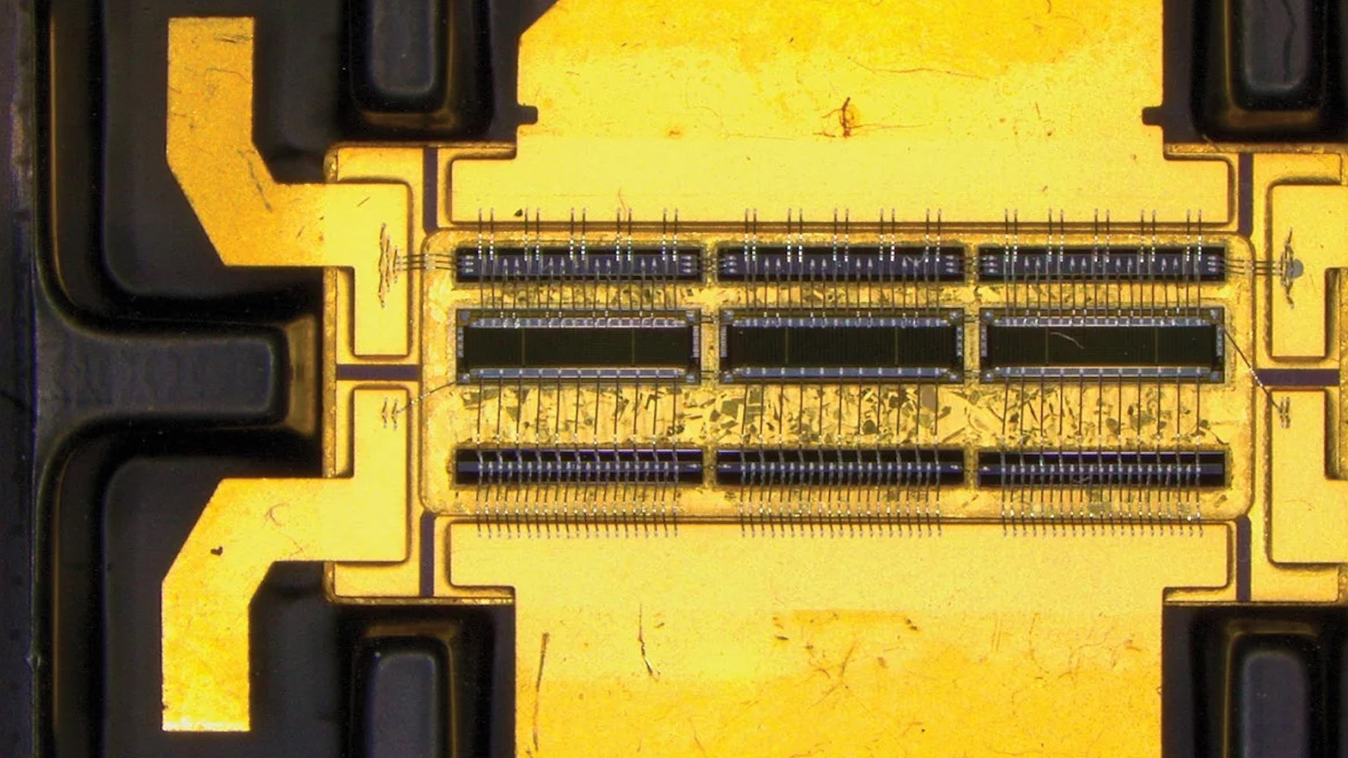
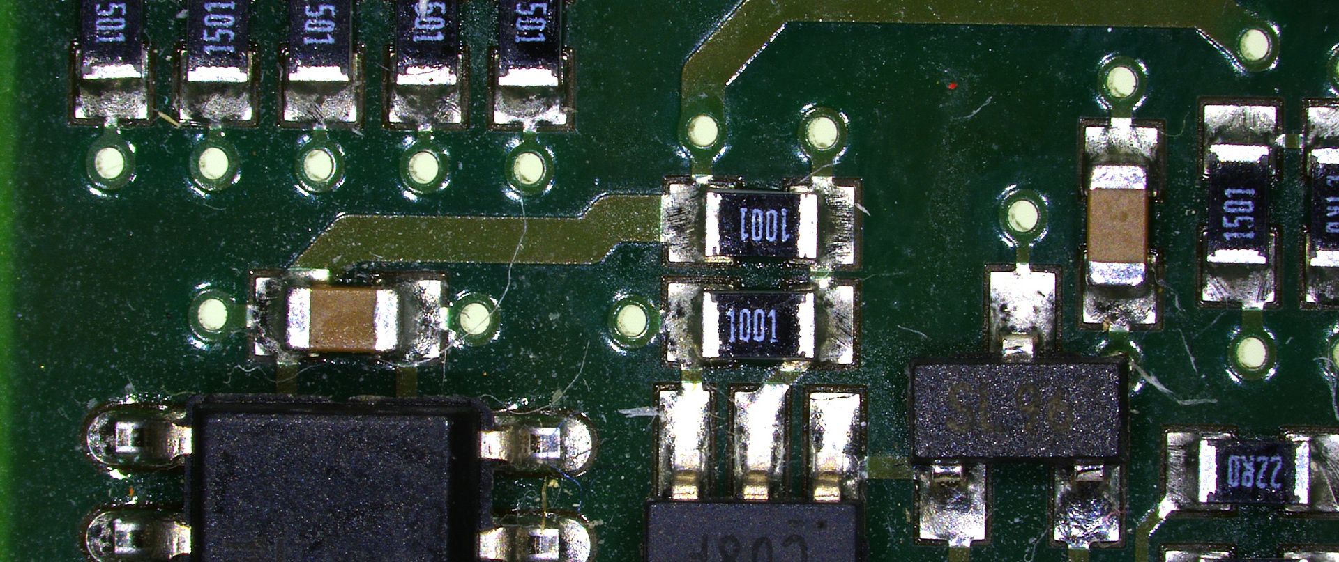
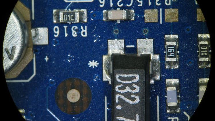
Inspecting and reworking solder joints is essential for device reliability. Leica rework microscopes enhance solder joint inspection and rework using FusionOptics, with its unique combination of high-resolution imaging and high depth of field high-contrast imaging. Glare reduction accessories also make it easier to spot irregularities and ensure solid connections.

Can large tools be used under the objective?
It is important to ensure you have enough space to work on your sample with various types of tools, such as soldering irons, during assembly and rework tasks. Leica assembly microscopes offer a working distance of up to 150 mm with a 0.63x objective lens and up to 200 mm with the auxiliary 0.5x lens.
Why use Leica microscopes for assembly and rework?
Leica Microsystems' Assembly microscopes provide several advantages that address the aforementioned challenges.
Optimal 3D perception
Less time spent adjusting the microscope means you can remain focused on the task at hand. FusionOptics is a technology that combines high resolution and greater depth of field at any zoom position for optimal 3D perception of samples.

Long working distance
Manipulate and work with your sample freely under the microscope. Long working distances of up to 200 mm (with the auxiliary 0.5x lens) allow for tools of various sizes to be used under the microscope.

Ergonomic design
The ergonomic design and wide variety of ergonomic accessories from Leica Microsystems reduces operator strain, allowing for longer periods of high-quality work.

Tailored for production
Tailored solutions with flexible arm configurations and various illumination options ensure precise, comfortable operation and highlight key sample features for specific applications.
Comparison table
A60 | Ivesta 3 | M80 | |||
| FusionOptics | Yes | Yes | No | ||
| Magnification range | Up to 30x | Up to 55x | Up to 60x | ||
| Working distance | Up to 122 mm | Up to 200 mm with the auxiliary 0.5x lens | Up to 107 mm (planachromatic) Up to 303 mm (achromatic) | ||
| Documentation | Not available | Optional with integrated or external camera + Enersight | Optional with Flexacam + Enersight | ||
| Ergonomy | 38° viewing angle is close to a person's natural head posture | 35° viewing angle | Wide range of ergonomic accessories to seamlessly fit multiple users, variable viewing angle 10°– 50° |
Related Articles
 at the edge of a battery electrode acquired with a DVM6 digital microscope.")
Burr Detection During Battery Manufacturing

Battery Particle Detection During the Production Process

Cross-section Analysis for Electronics Manufacturing

Rapid and Reliable Examination of PCBs & PCBAs with Digital Microscopy
Frequently asked questions Assembly & Rework Microscopes
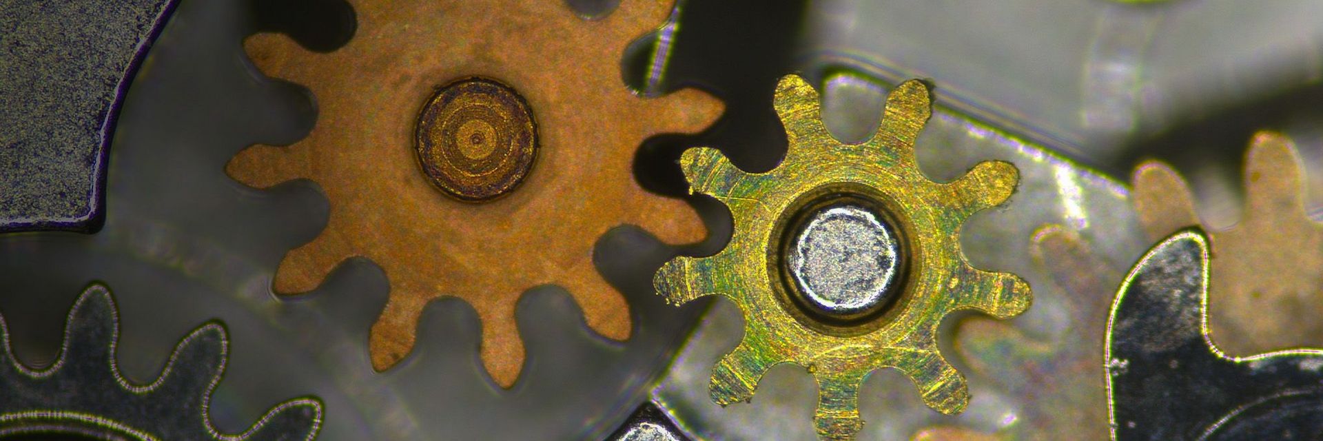
Leica assembly microscopes, with their comprehensive illumination options, can be used for a great variety of sample types in the electronics (e.g. PCB), medical device (e.g. stents, catheters, pacemakers, hearing aids) or the watchmaking industry.
Leica cameras enable immediate image documentation during the assembly process. They can be networked or used in standalone mode.
Leica Microsystems offers extensive support services, including regular maintenance and calibration, to ensure that their microscopes continue to operate throughout lifetime at peak performance, safeguarding the quality and reliability of your assembly processes.
Yes, Leica microscopes are designed to meet cleanroom and ESD protection standards, making them suitable for sensitive environments like semiconductor and medical device manufacturing. The A60 microscope has a grounding point at the back of the base plate, and ESD stands are available for the Ivesta and M series microscopes.
With our easy-to-use systems and software, users can be up and running quickly. With an adaptable user interface, unnecessary functions for the user’s required task can be hidden, making the user interface as lean as you desire to minimize training time.
Yes, Leica microscopes are designed for easy integration into various assembly lines, and offer different options for stands, arms, etc. allowing maximum compatibility for integration in production environments.
Choose a microscope for PCB rework with high magnification, large depth of field, and excellent illumination for detailed inspection. Look for ergonomic design, flexible positioning, and digital imaging options. Ensure it supports steady, accurate manipulation of components during intricate and time-consuming repair tasks.
Common PCB rework challenges involve identifying microscopic defects, precisely removing or replacing components, and inspecting complex connections. A microscope can help ensure accurate alignment, minimize damage during repairs, enhance visibility in tight areas, and improve handling efficiency.
PCB rework involves repairing or modifying a printed circuit board to fix defects, replace components, or update older designs. It's needed to fix faulty boards, address manufacturing errors, or upgrade functionality, thereby reducing waste and ensuring better product reliability.
Choose a microscope for PCB assembly by prioritizing high magnification, wide field of view, and adjustable focus. Look for good illumination options, ergonomic design, and flexibility in positioning and stability. Consider digital capabilities for documentation and ensure the microscope meets your specific assembly and inspection needs.
Common PCB assembly challenges include inspecting microscopic components, identifying soldering defects, and aligning intricate parts. A good assembly microscope provides magnification, clear illumination, specifically glare reduction, and precision, enabling accurate inspection, defect detection and depth of field, and alignment and ensuring high-quality assemblies.