


 and phalloidin (magenta), imaged using Viventis SCAPE; scale bar 50μm. Courtesy of Marina Cuenca and Heleen Jungen (Dayton lab), EMBL Barcelona.")

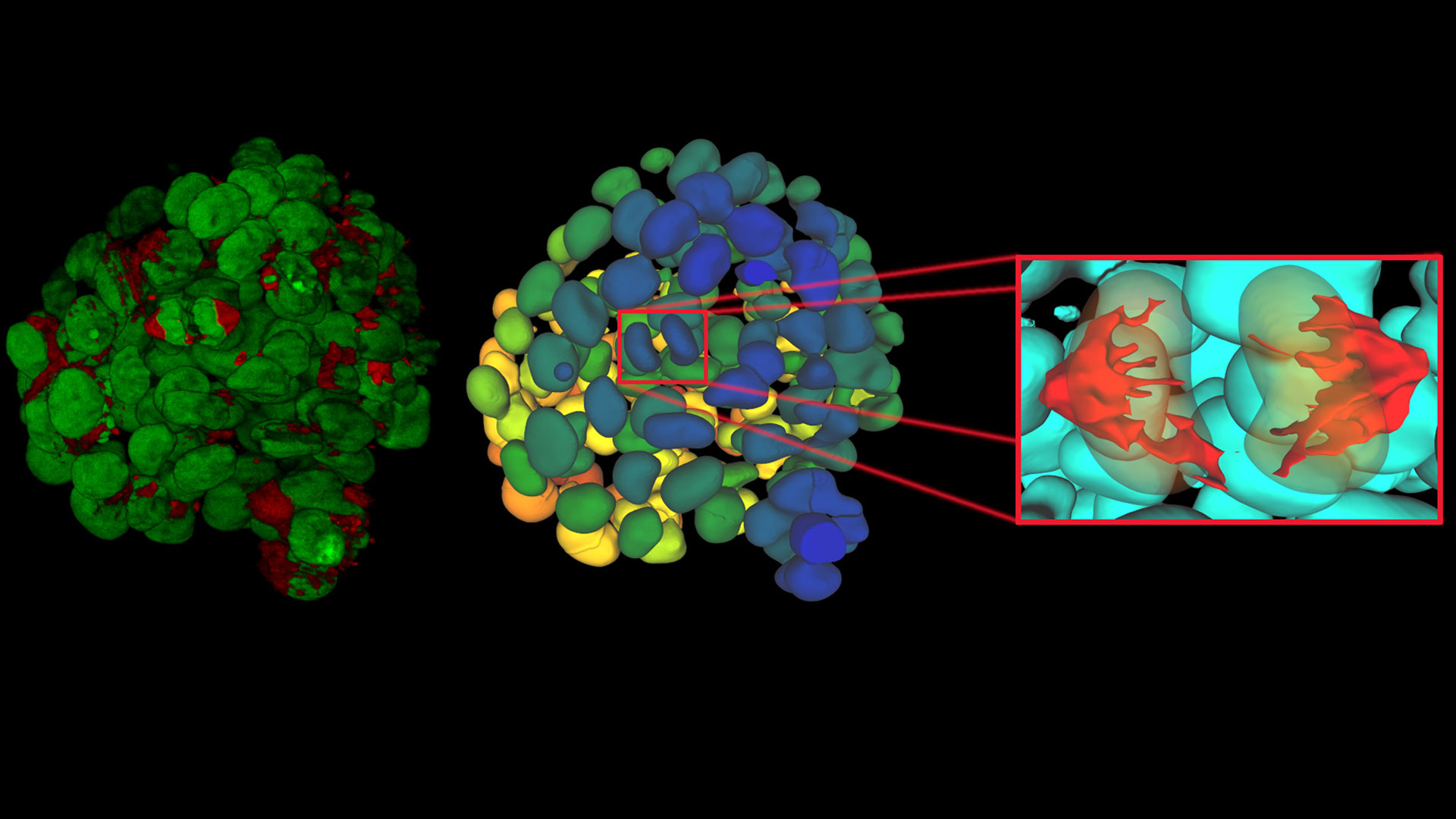
 2D slices of a 1 mm diameter midbrain neural organoid stained with DAPI (blue, nuclear stain), β-tubulin (green, neuronal stain), and GFAP (red, astrocyte stain).")


 and acceptor (A) molecule which participate in FRET (Förster resonance energy transfer).")


Software enhancements help researchers simplify complex studies and generate results with confidence
Our Latest Articles
What’s the Best Organoid Imaging Approach for Early Drug Discovery?
Organoids and other complex in vitro models (CIVMs) are becoming increasingly important in early drug discovery and translational research, driven by the need for more predictive, human-relevant data…
Waffle Method Workflow: From HPF to Cryo-ET Lamellae
Waffle freezing provides an HPF-based route to cryo-ET sample preparation. This workflow guide follows the process from grid and carrier assembly to vitrification, cryo-FIB milling, lamella…
Fast, High-Contrast Widefield Imaging of Optically Challenging Samples
Live‑cell imaging of large, complex biological samples often requires large fields of view, sub-cellular resolution, high-sensitivity, and fast acquisition – all while maintaining low illumination…
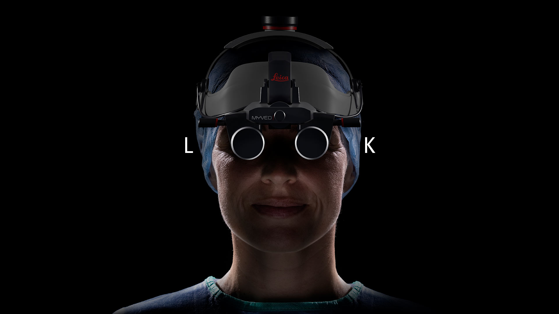
Dental Loupes vs Microscopes: Exploring Visualization Options in Dentistry
Dental professionals often ask: “Should I use dental loupes or invest in a microscope?” This article explores the key differences between dental microscopes and dental loupes, focusing on…
Spatial Proteomics Workflow in Blood Cancer (MPNs)
Megakaryocytes play a central role in the biology of myeloproliferative neoplasms (MPNs), yet their in vivo proteomic characterization remains a major challenge due to low abundance and disrupted…
Six Features to Consider when Choosing a Dental Microscope
The dental surgical microscope has become increasingly important for high-quality and successful dental medicine, particularly in the field of endodontics. A dentist can conduct micro-invasive…
Multiscale Imaging of Organoids: High Content to Light Sheet
Learn multiscale organoid imaging: fixed high content phenotyping, gentle dual view light sheet, and reproducible pipelines that turn 3D data into insights.
What is FRET with FLIM or as it is usually known FLIM-FRET?
Förster resonance energy transfer (FRET) is a well-established fluorescence-based technique which is used to study molecular interactions. It is useful for the analysis of protein-DNA and…
Ratiometric Imaging and Analysis of Ion Concentration in Cells
Many cellular functions depend on the dynamic balance of ions, electric potentials, and pH between the cytosol and surrounding extracellular space. Changes in these values affect cellular function.…
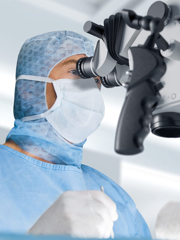
4 Key Benefits of 3D Digital Microscopy in Ophthalmic Surgery
3D digital visualization is rapidly transforming ophthalmic surgery. Modern 3D surgical microscopes enable surgeons to perform procedures using high-resolution digital displays rather than traditional…
ATTO-TEC Consumables
ATTO-TEC dyes have become a benchmark for fluorescence microscopy imaging, offering a highly differentiated panel. Their brightness and photostability make them the reagents of choice for demanding applications.

The Viventis Deep light sheet microscope supports both live and cleared imaging on one configurable platform

Customers gain access to microscopy solutions, software, and localized purchasing options in their local languages

The Launch Early Access Program (LEAP) from Leica Microsystems provides supported access to the ATTOAuriga reagent platform

Leica Microsystems launches the Viventis SCAPE light sheet microscope. It enables fast 3D light sheet imaging while using standard sample carriers.…
