
Science Lab
Science Lab
Das Wissensportal von Leica Microsystems bietet Ihnen Wissens- und Lehrmaterial zu den Themen der Mikroskopie. Die Inhalte sind so konzipiert, dass sie Einsteiger, erfahrene Praktiker und Wissenschaftler gleichermaßen bei ihrem alltäglichen Vorgehen und Experimenten unterstützen. Entdecken Sie interaktive Tutorials und Anwendungsberichte, erfahren Sie mehr über die Grundlagen der Mikroskopie und High-End-Technologien - werden Sie Teil der Science Lab Community und teilen Sie Ihr Wissen!
Filter articles
Tags
Berichtstyp
Produkte
Loading...
 and oblique (right) brightfield illumination using a Leica compound microscope. The defect on the wafer surface is clearly more visible with oblique illumination.")
Rapid Semiconductor Inspection with Microscope Contrast Methods
Semiconductor inspection during the production of patterned wafers and ICs (integrated circuits) is important for identifying and minimizing defects. To increase the efficiency of quality control in…
Loading...

How to Successfully Perform Live-cell CLEM
The Leica Nano workflow provides a streamlined live-cell CLEM solution for getting insight bout structural changes of cellular components over time. Besides the technical handling described in the…
Loading...
Capture life as it happens
With the Leica Nano Workflow, searching for the needle in the haystack is a thing of the past. Take advantage of correlative light and electron microscopy to identify directly the right cell at the…
Loading...
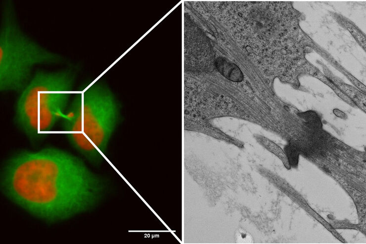
Investigating Synapses in Brain Slices with Enhanced Functional Electron Microscopy
A fundamental question of neuroscience is: what is the relationship between structural and functional properties of synapses? Over the last few decades, electrophysiology has shed light on synaptic…
Loading...

Microscopy in Virology
The coronavirus SARS-CoV-2, causing the Covid-19 disease effects our world in all aspects. Research to find immunization and treatment methods, in other words to fight this virus, gained highest…
Loading...

Top Issues Related to Standards for Rating Non-Metallic Inclusions in Steel
Supplying components and products made of steel to users worldwide can require that a single batch be compliant with multiple steel quality standards. This user demand creates significant challenges…
Loading...

Analyzing Non-metallic Inclusions in Steel
Oftentimes we find ourselves caught up in tedious analyses by reticle and comparison chart, time-consuming double-evaluation according to several standards or subjective inspection results with a bias…
Loading...
")
Performing Elemental Analysis down to the Micro Scale
If you work in electronic component analysis, you will be familiar with the many challenges posed. Whether you are identifying metallic particles or checking product authenticity, it’s important to…
Loading...
Introduction to Ion Beam Etching with the EM TIC 3X
In this article you can learn how to optimize the preparation quality of your samples by using the ion beam etching method with the EM TIC 3X ion beam milling machine. A short introduction of the…
