
Science Lab
Science Lab
Das Wissensportal von Leica Microsystems bietet Ihnen Wissens- und Lehrmaterial zu den Themen der Mikroskopie. Die Inhalte sind so konzipiert, dass sie Einsteiger, erfahrene Praktiker und Wissenschaftler gleichermaßen bei ihrem alltäglichen Vorgehen und Experimenten unterstützen. Entdecken Sie interaktive Tutorials und Anwendungsberichte, erfahren Sie mehr über die Grundlagen der Mikroskopie und High-End-Technologien - werden Sie Teil der Science Lab Community und teilen Sie Ihr Wissen!
Filter articles
Tags
Berichtstyp
Produkte
Loading...

Automotive Part Verification and Development according to Specifications
Automotive part verification during the development and production of parts and components by suppliers or manufacturers is important for ensuring that specifications are met. Specifications are…
Loading...
A Guide to Darkfield Microscopes
A darkfield microscope offers a way to view the structures of many types of biological specimens in greater contrast without the need of stains.
Loading...
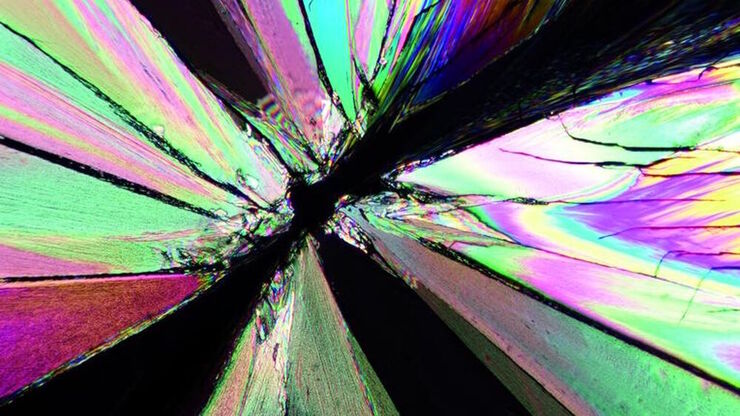
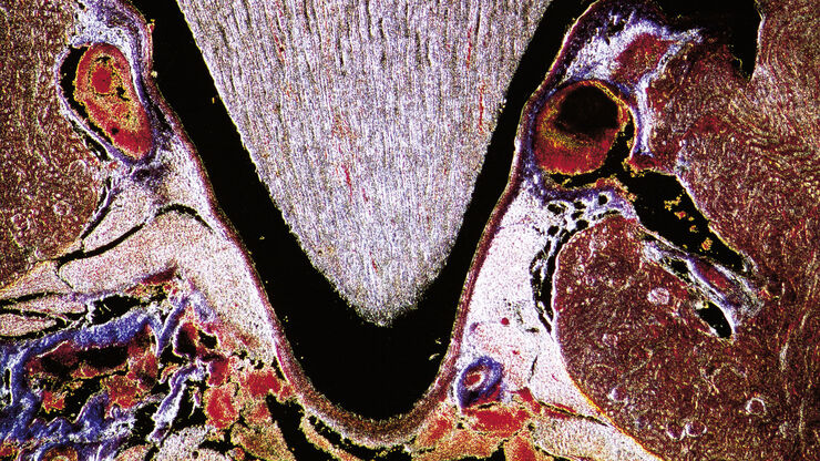
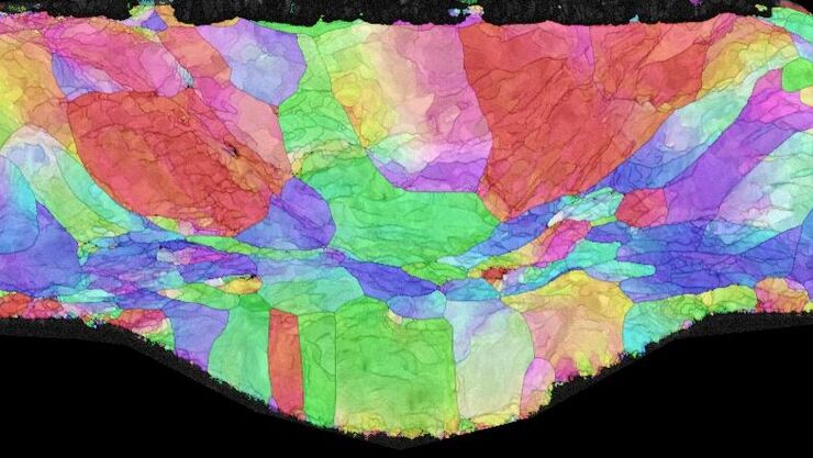
Das Prinzip der Polarisationsmikroskopie
Die Polarisationsmikroskopie wird in den Material- und Geowissenschaften routinemäßig eingesetzt, um Materialien und Mineralien anhand ihrer charakteristischen Brechungseigenschaften und Farben zu…
Loading...
. With DIC users are able to visualize small height differences on the wafer surface more easily.")
6-Inch Wafer Inspection Microscope for Reliably Observing Small Height Differences
A 6-inch wafer inspection microscope with automated and reproducible DIC (differential interference contrast) imaging, no matter the skill level of users, is described in this article. Manufacturing…
Loading...

Visualizing Photoresist Residue and Organic Contamination on Wafers
As the scale of integrated circuits (ICs) on semiconductors passes below 10 nm, efficient detection of organic contamination, like photoresist residue, and defects during wafer inspection is becoming…
Loading...
Workflow Solutions for Sample Preparation Methods for Material Science
This brochure presents and explains appropriate workflow solutions for the most frequently required sample preparation methods for material science samples.
Loading...

Technical Terms for Digital Microscope Cameras and Image Analysis
Learn more about the basic principles behind digital microscope camera technologies, how digital cameras work, and take advantage of a reference list of technical terms from this article.
Loading...
 and oblique (right) brightfield illumination using a Leica compound microscope. The defect on the wafer surface is clearly more visible with oblique illumination.")
Rapid Semiconductor Inspection with Microscope Contrast Methods
Semiconductor inspection during the production of patterned wafers and ICs (integrated circuits) is important for identifying and minimizing defects. To increase the efficiency of quality control in…
Loading...

Cross-section Analysis for Electronics Manufacturing
This article describes cross-section analysis for electronics concerning quality control and failure analysis of printed circuit boards (PCBs) and assemblies (PCBAs), integrated circuits (ICs), etc.
