A clean section
The first step is always to produce a polished metallographic section. However, the preparation of the real microstructure is only successful if the surface of the sample is completely clean and deformationfree. After the section has been produced it is normally immediately etched in acids, lyes or salt solutions to develop the microstructure. This attacks the grain boundaries or roughens certain grain and phase areas which then appear dark in brightfield.
Combining the right methods
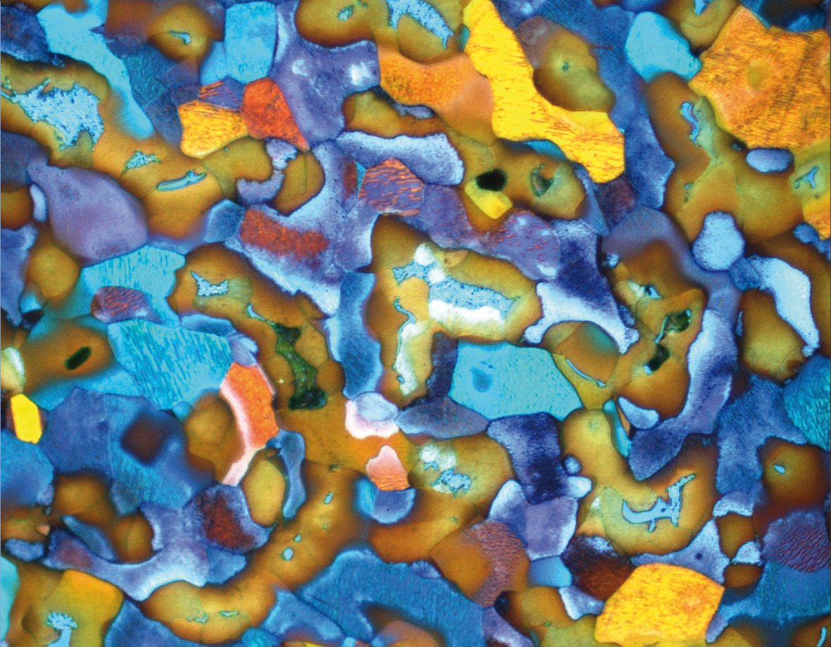
If these techniques are not sufficient to allow a full examination, if the etching result does not meet the specifications or if the material is etch-resistant, either color etching or other light microscopic techniques such as polarization, darkfield and interference contrast are used. Often, it takes a combination of color etching and optical contrasting to get the best results. The great variety of possible imaging techniques is shown by the photos of the same detail of a copper alloy sample (Figures 1–6).
Figures 7 to 12 show different ways of contrasting microstructural constituents in different materials. The color etching technique applied here caused the formation of sulphate layers of different thicknesses on the grain or mixed crystal areas.
The sections were etched in Klemm (K) or Beraha (B) etchants, which are tint etches based on potassium sulphite. The composition is given in "Metallographisches, keramographisches, plastographisches Ätzen" by Günter Petzow and Veronika Carle, published by Borntraeger, 2006. In Figures 7 and 8, the ferrite in the steel is colored, while the iron carbide is kept white to achieve a clear contrast of the carbide precipitations. Weld layers of austenitic steel are shown in Figures 9 and 10. The images highlight not only the cast structure, but also the segregation and heataffected zones. Figure 11 also shows a segregation in a tin bronze sample due to incipient melting. Figure 12 is a good example of how such an etching can even be used to visualize subgrain formation.
Figs. 7–9 (from left to right): Color etching of various grain or mixed-crystal areas and sulphate layers of different thicknesses:
Fig. 7: Ferrite-perlite microstructure, the ferrite is tinted while Fe3C is kept white Klemm (K) etch
Fig. 8: This contrasting visualizes the quality of a soft annealing (K)
Fig. 9: Microstructure of an austenitic cast produced by laser treatment, Beraha (B) etch
Figs. 10–12 (from left to right): Color etching of various grain or mixed-crystal areas and sulphate layers of different thicknesses:
Fig. 10: Laser welding connection of various austenitic steel wires (B)
Fig. 11: Concentration differences in a bronze wire (K)
Fig. 12: Grain area etching and subgrain formation in a tin rod
Polarization with and without color etching
Color contrast and specific microstructure formations can frequently be enhanced by optical polarization of the etched samples under the microscope. In Figures 13–18, this method is used to highlight different deformation mechanisms (mainly induced in the manufacture of semi-finished products or components) and ensuing specific deformation structures in the material microstructure.
Figs. 16–18 (from left to right): Polarization with and without color etching:
Fig. 16: SnPb tin solder, twinning shows deformation at the solder point (K)
Fig. 17: Sn dynamically deformed, the pronounced formation of deformation twinning is a sign of a dynamic load (K)
Fig. 18: Slip bands due to pronounced deformation on a CuZn wire with fcc lattice (K).
The examination of the sample in polarized light is also often helpful in cases where color etching fails to provide the desired contrast of individual microstructure components, or if only one phase is attacked in composite materials. Examples are shown in Figures 19 to 21. Figure 19 shows a much better image of the grain and twin structure in a 10 cent coin made of Nordic gold, while in Figure 20, individual crystals and their needle structure can be seen in tungsten carbide. Figure 21 shows the amount, size and shape of graphite fibers in black, carbon fiber reinforced plastic. If documentation is required of the different components of a composite material, additional optical contrasting is usually essential. Figure 22 documents the excellent result that can be achieved by optical imaging of the microstructure of special brass and, at the same time, the glass fiber braid coating. In the photo of a severed capacitor, the glass fiber core can be seen in its thin copper sleeve welded onto a conductor track of tin bronze (Figure 23). The last photo of this series shows an anti-wear sintered layer of tin bronze with graphite components and ceramic particles (Figure 24).
These examples clearly demonstrate that the distribution and formation of different phases are of great, if not overriding, significance for the properties of the material. This is why clear differentiation with the method presented here is particularly important.
Figs. 19–21 (from left to right): Polarization with and without color etching:
Fig. 19: 10 eurocent coin made of Nordic gold (K)
Fig. 20: Structure of a cast tungsten carbide W2C consisting of a needle structure, etchpolished with H2O2 and polarized
Fig. 21: Carbon fibers in a structural component, made of carbon fiber-reinforced plastic unetched, polarized
Figs. 22–24 (from left to right): Polarization with and without color etching:
Fig. 22: Brass component with bonded glass fiber braid (K)
Fig. 23: Capacitor with plastic – glass fiber core, copper-plated and soldered onto a bronze strip conductor (K)
Fig. 24: Sintered wear protection coating containing bronze and graphite and ceramic particles, clearly visible deformation in the bronze through the calibration (K)
Contrasting with interference
Figures 25 to 28 show that a microstructure that has already developed due to etching reveals an additional dimension when imaged in interference contrast. This is particularly noticeable in the cast brass wire shown below (Figure 27), where the crystal structure and also the dendritic solidification typical of a cast can be seen in far greater detail.
Figs. 25–28 (from top left to bottom right): Improved contrast using interference:
Fig. 25: Brightfield image of a cast austenite structure caused by a laser melting process
Fig. 26: The same sample in interference contrast showing clear contrasting of the dendrites (B)
Fig. 27: Center of a brass wire rod in brightfield
Fig. 28: The same sample in interference contrast with significantly better grain contrast and visualization of dendrites and their direction of solidification (K)
Figures 29 to 31 are further impressive examples of the potential of interference contrast imaging. Figure 29 shows the material behavior of tin, in which sudden stress leads to new grain formation and crystalline Umklapp processes due to twinning. Figure 30 clearly shows the orientation of slip bands in the grain microstructure in accordance with the grain orientation. This technique can be used for most etch-resistant hard metals to obtain a much better image of spherolithic carbides with their secondary adhesions – here embedded in a two-phase nickel-based alloy (Figure 31).
Combinations of extremely different substances in one material are illustrated in Figures 32–34. Figure 32 shows a silver solder ceramic/copper connection. Figure 33 depicts a composite of glass-plastic layer and glass fiber braid coating stuck to a ceramic substrate. A cross-section of an electronic component can be seen in Figure 34, with the glass fiber-reinforced plastic on one side of the copper conductor and the ceramic structure on the other.
Figs. 29–34 (from top left to bottom right): Examples of contrast enhancement using interference for samples with and without color etching:
Fig. 29: Deformation twinning generated by abrupt reforming (K)
Fig. 30: Contrasting of the slip bands in a deformed copper bronze sample (K)
Fig. 31: A good image of the cast tungsten carbides in the nickel matrix is achieved with interference contrast
Fig. 32: Silver solder in copper/ceramic compound (etch-polished + K)
Fig. 33: Cross-section view of a circuit board, composite of different plastics, polished
Fig. 34: Cross-section view of an electronic component, ceramics, metal and glass-fiber reinforced plastic (B)


