
As the size of semiconductor patterning is getting smaller and the number of integrated circuits (ICs) produced is getting greater, residual contamination on wafers during manufacturing becomes more troublesome when attempting to meet quality standards. Therefore, keeping wafers clean during production is critical.
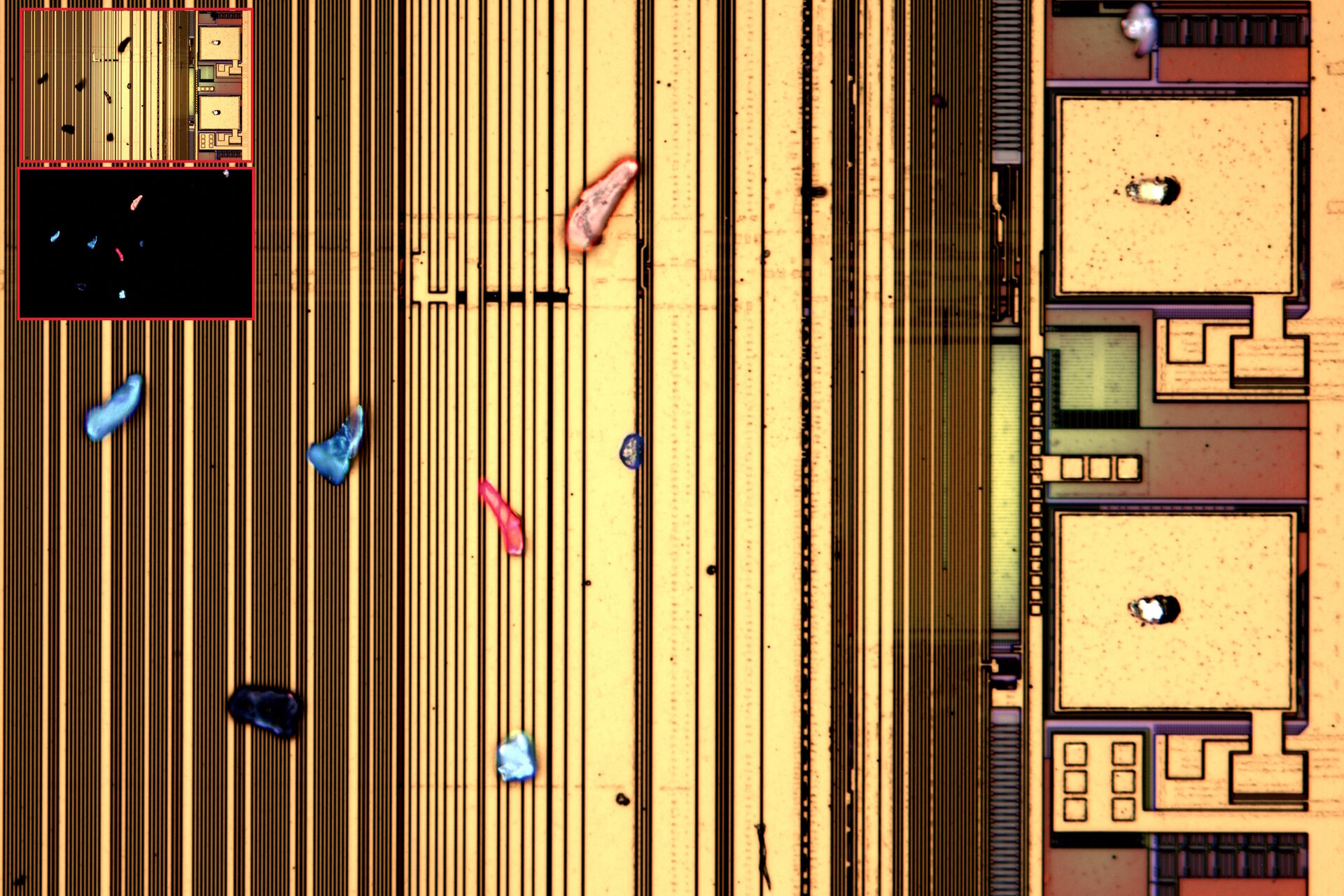
Contamination on wafers can be photoresist residue, foreign organic particles and liquids, dust, fibers, and human hair and skin. Wafer inspection is often done with optical microscopy for efficient visualization of even small amounts of contamination during production. To see organic contamination, fluorescence microscopy has advantages compared to more common illumination methods like brightfield or darkfield.
This article demonstrates how fluorescence microscopy can be used to:
- Efficiently visualize organic contamination during wafer quality control (QC) leading to reduced inspection times, higher throughput, and improved semiconductor component quality.
- Reliably and rapidly monitor the quality of the RGB array output for OLED (organic light emitting diode) flat panel displays.
By taking advantage of multiple contrast and illumination techniques, including fluorescence, and a large magnification range, users can meet their specific needs for inspection, QC, failure analysis, and research and development (R&D) of wafers and semiconductor materials with Leica microscopes like the DM8000 M, DM12000 M, or DM6 M.
To read the article and find out more, just fill in the form below.
. With DIC users are able to visualize small height differences on the wafer surface more easily.")
 and oblique (right) brightfield illumination using a Leica compound microscope. The defect on the wafer surface is clearly more visible with oblique illumination.")
 chip cross section acquired at higher magnification showing a region of interest.")