EM TIC 3X Ion Beam Milling Machine
The EM TIC 3X is a broad ion beam milling unit that is used to prepare sample cross sections as well as planar samples for scanning electron microscopy (SEM), light microscopy (LM), microstructure analysis (EDS, WDS, Auger, EBSD) and atomic force microscopy (AFM) investigations. The instrument is equipped with a triple ion beam system and can process large surface areas of almost any material at room temperature or cryo.
The EM TIC 3X is setup as a modular system and can be flexibly equipped with different stages for various applications:
- Standard stage: prepare a wide range of samples with different sizes, shapes and materials
- Cooling stage: prevents thermally-cooling sensitive samples from being destroyed by overheating
- Multiple sample stage: prepare at least three samples successively without user interaction guaranteeing a high-level sample throughput.
- Rotary stage: for flat milling or ion beam polishing
To learn more about the EM TIC 3X Ion Beam Milling Machine visit:
The ion beam etching method
Ion Beam Etching, also known as Ion Beam Milling or Ion Milling, is the most widely-used etching method for preparing solid state samples for scanning electron microscopy (SEM) applications. In this process, the sample material is bombarded with high-energy argon ion beams in a high vacuum chamber. The top layer of the material is removed by high energy ions to achieve a defect-free sample surface. The ion energy and milling angle depend on the corresponding application and can be adjusted accordingly. It is also possible to improve the quality of mechanically polished surfaces via a final ion polishing process. The surfaces of samples can be cleaned, polished and have their contrast enhanced using ion milling techniques. These techniques are used to obtain high resolution SEM images for various applications such as failure analysis and to perform surface sensitive analyses such as EBSD for material characterization.
The working principles of the EM TIC 3X unique triple ion beam system
The triple ion source of the EM TIC 3X consists of three independent controllable saddle-field ion guns. The ion energy is adjustable between 1 to 10 keV. The ion source will be fed with a process gas, preferably Argon. A high voltage (1 to 10 kV) will be applied on the anode. The cathodes and Wehnelt cylinders are on earth potential. Due to the electrical field between anode and cathode the process gas will be ionized (Ar+) and the plasma ignites. Positive charged ions will be accelerated towards the cathodes and generate electrons. This bombardment leads to an abrasion of the cathode. Negative charged electrons will be accelerated towards the anode and collide with gas atoms and generate ions. Due to the shape of the electrical field between anode and Wehnelt cylinders (saddle field) two ion beams are created and accelerated towards both cathodes. One beam is blocked by the (blind) rear side cathode. The other beam will be led through the beam exit at the front side cathode. The energy of the ions coming out matches the acceleration voltage.
Cross section sample preparation by ion beam etching
To produce cross sections for scanning electron microscopy (SEM), the sample is covered with a sharp-edged mask such that only 50–100 µm of the sample material is exposed above the mask. The three ion beams intersect at the center of the mask edge and strike the uncovered material and remove it to produce a sample cross-section with a high surface quality. The design of the ion gun develops a milling rate of 300 μm/hour (Si 10 kV, 3.5 mA, 100 μm from edge). This unique technique produces a vast cross sectioning area of larger than 4 × 1 mm at a high material removal rate to achieve a high-quality surface finish.
Planar sample preparation by ion beam etching
For flat milling (or ion beam polishing) the rotary stage is used. Due to the gun assembly and additional lateral movement of the sample, a uniform, high quality area larger than 25 mm diameter can be prepared.
This preparation process is used to clean, polish or enhance the contrast of a mechanically or chemically polished surface with the goal of removing fine scratches, abrasive material and smearing artifacts.
Examples of samples polished with the EM TIC 3X ion beam milling machine
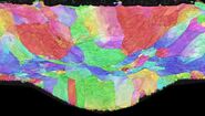
ZINC ON STEEL: Zinc is very soft compared to steel and would become smeared during mechanical polishing. Ion milling is a known technique to analyze the thickness of zinc layer on galvanized steels. After using the EM TIC 3X, a cleanly etched surface can be observed. The zinc layer is free of artifacts and the grain structure as well as interface layer are clearly visible.
SOLDER BUMP: The semiconductor structure with solder bumps is a very soft material that is rarely prepared successfully using conventional mechanical polishing. Ion beam milling is the preferred method of preparing such samples. To avoid shrinkage of the individual components in the solder bump, the sample was protected by liquid nitrogen and kept cool during ion milling. Results show a smooth and clean surface and the structural details in the solder bump are easily recognizable.
Further reading
- Workflow Solutions for Industrial Research
- Sample Preparation for Electron Microscopy
- Application Booklet EM TIC3X
- Workflow Brochure Life Science


