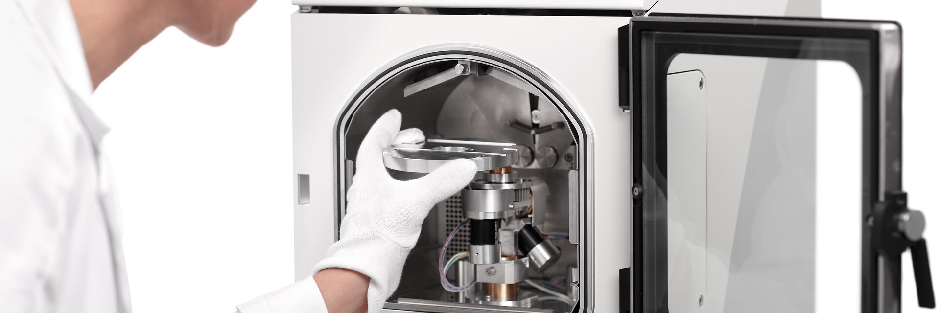
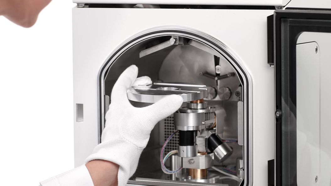
Coating
A sample is coated with either a conductive layer of carbon or metal to inhibit charging, to reduce thermal damage and to improve the secondary electron signal for topographic examination in the SEM. For TEM analysis of samples, carbon coated grids are used or the sample itself might need a thin layer of coating on top. Leica Microsystems’ coater line comprises the Leica EM ACE600 high vacuum coater for highest resolution analysis in FE-SEM and TEM and the Leica EM ACE200 sputter and/or carbon thread coater as a fully automated system for fast, convenient and intuitive handling.
Why do I need to coat my samples for electron microscopy (EM)?
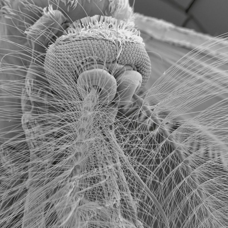
For EM imaging, a sample which is not inherently conductive must then be coated with a conductive layer to inhibit the risks of charging and thermal damage to the sample. In some cases, thin metal films also help to improve the secondary electron emission signal.
Related articles
Brief Introduction to Coating Technology for Electron Microscopy

Coating techniques
The most appropriate coating technique to use depends on your sample’s properties, the size of the structures you like to analyze, and the methods needed to prepare it for EM imaging. For some advanced applications, you have to freeze fracture and possibly freeze etch your samples. In that case you need an instrument which has the capability of cold transfer, coating the sample under cryogenic conditions, and fracturing the sample with a cryo knife.
From coatings done in a low-vacuum sputter coating machine at room-temperature to those done in high-vacuum and even at cryogenic temperatures, Leica coating solutions cover a large range of needs. Instruments are designed to improve and optimize your sample preparation workflows from basic coatings to the most advanced freeze fracture applications.
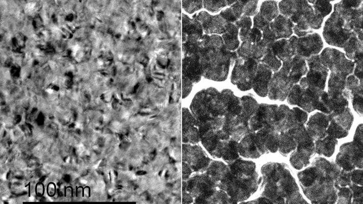
What is the difference between coatings prepared with a high-vacuum or low-vacuum sputter coater?
The vacuum conditions have a significant impact on the thin film quality.
Low-vacuum sputter coaters
allow thin film deposition for SEMapplications with moderate magnification demands. Samples can be sputter coated with gold (Au) as well as other suitable materials like platinum (Pt) and gold/palladium (Au/Pd).
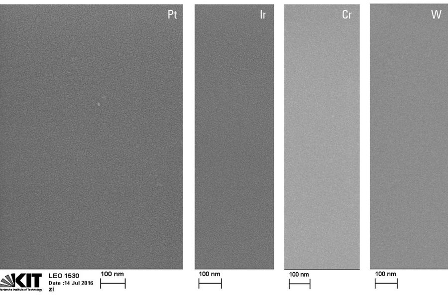
High-vacuum sputter coaters
deposit thin films with much finer grain structure allowing for high-resolution SEM analysis. Also, a broader range of materials, including oxidizable metals, can be sputtered. Examples are iridium (Ir), tungsten (W), or titanium (Ti). Sometimes chromium (Cr) is sputtered to form a buffer layer. In addition, high-vacuum coaters can be configured for more advanced applications and multi-layer deposition.
Sputter coating
During the sputter coating process, a plasma of Argon (Ar) ions is formed in front of a metal target. Ar ions are accelerated towards the target, guided by a magnetic field. Once the Ar ions impact the target, small fragments of target material will be released. These small fragments travel towards the sample and build up, forming a thin film of material over time. The quality of the thin film depends on the deposition rate and other sputter process parameters.
RF and DC Sputtering
Sputter coaters for EM sample prep involve DC (direct current) sputtering. DC sputtering is suitable for conductive materials. Other more advanced sputter coating machines include also radio frequency (RF) sputtering using an AC (alternating current) field which prevents charge buildup on the sample surface. RF sputtering allows sputtering of oxides and other non-conductive materials.
Carbon coating
Carbon (C) films are conductive and transparent to an electron beam. They can be thin, but still strong. TEM grid support films are often made from carbon. Coating a material with carbon involves the thermal evaporation of carbon. The carbon source is normally in the form of a thread. Heating of the carbon can be done either by running a current through the C-thread or by electron bombardment (e-beam evaporator). When the carbon source is heated to its evaporation temperature, a fine stream of carbon strikes the sample. The end result is that the sample becomes coated with a layer of carbon.
When should I coat with carbon?
Carbon (C) coatings are commonly used as a support film for transmission electron microscopy (TEM). Thin films of carbon are typically a few nanometers thick and deposited onto TEM grids. They are thin, strong, and transparent to electrons. A carbon coating is also used as a protective layer.
How is something carbon coated?
Carbon (C) films are conductive and transparent to an electron beam. They can be thin, but still strong. TEM grid support films are often made from carbon. Coating a material with carbon involves the thermal evaporation of carbon. The carbon source is normally in the form of a thread. Heating of the carbon can be done either by running a current through the C-thread or by electron bombardment (e-beam evaporator). When the carbon source is heated to its evaporation temperature, a fine stream of carbon strikes the sample. The end result is that the sample becomes coated with a layer of carbon.
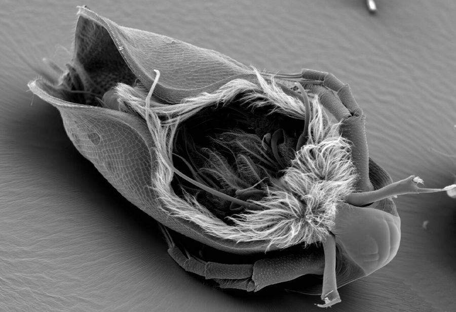
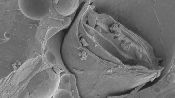
Freeze fracture
To reveal internal structures of a frozen specimen, it can be physically broken to expose those structures for examination with an electron microscope. The Leica EM ACE900 cryo coater brings the freeze fracture technique to a new level, featuring an advanced microtome, flexible shadowing options with electron beam sources, a rotating cryo stage and a load-lock transfer system. High resolution analysis of replicas in the TEM and, equipped with the Leica EM VCT500, block face imaging in the cryo SEM are the results of this technique. The Leica EM ACE600 equipped with a cryo stage and a VCT500 connection provides a solution for freeze fracturing to image the revealed surface in a cryo SEM.
For which applications is freeze fracture used?
To reveal the internal fine structures of a biological or organic specimen, the specimen can be cooled to cryogenic temperatures and physically broken. Once coated with a conductive layer, the exposed fine structures of the specimen can then be examined with electron microscopy (EM). Freeze fracture is traditionally used for biological applications, like the investigation of subcellular structures, e.g., organelles and membranes. However, more recently the technique has become interesting for certain applications in materials science and physics concerning layers and emulsions.
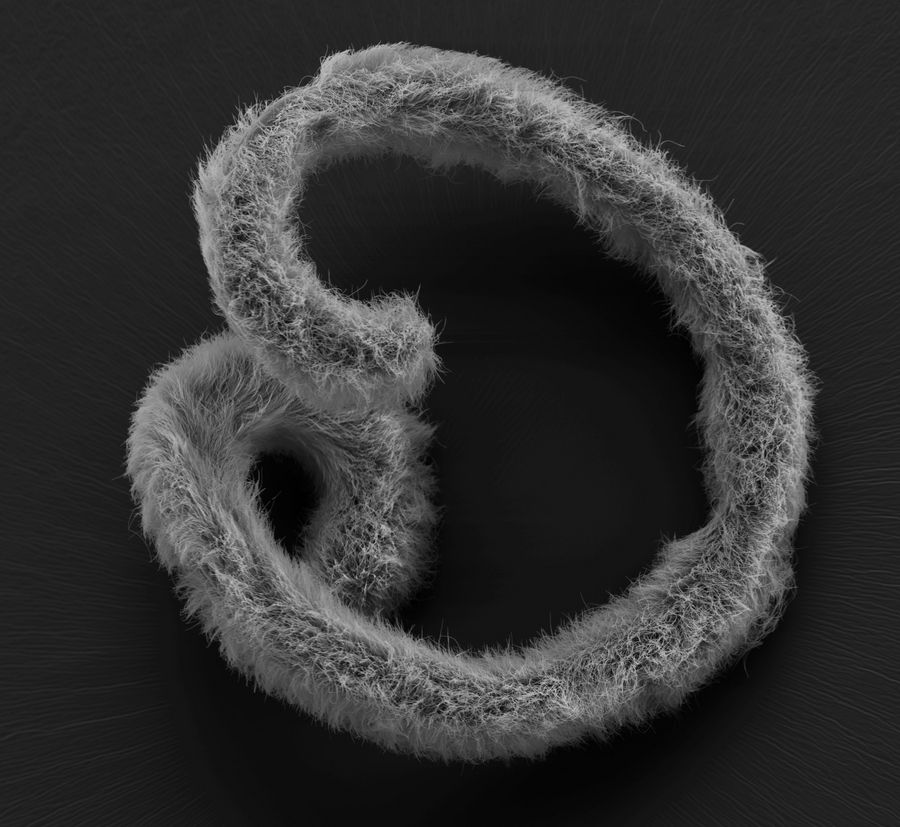
Freeze etching
Freeze etching is an optional step after freeze fracturing the sample and reveals more information from the fractured faces. This is achieved by sublimating superficial ice layers under vacuum to expose cellular elements that were originally hidden. Stage temperature and vacuum are influencing the etching rate. Accurate temperature control of the stage is required to achieve reproducibility. As a highly versatile instrument the Leica EM ACE900 cryo coater offers best results for freeze fracture and freeze etching techniques for TEM, and cryo SEM analysis.
Related articles

Brief Introduction to Freeze Fracture and Etching
Improvement of Metallic Thin Films for HR-SEM by Using DC Magnetron Sputter Coater
Frequently asked questions Sputter Coating & Freeze Fracture
The coating solution is shipped in the configuration that best fits your stated needs or application. In case your needs change later, you can always ask your local Leica sales representative about available accessories for upgrading your coating solution.
There are a lot of accessories. Please get in contact with your local Leica sales representative.


