
Science Lab
Science Lab
The knowledge portal of Leica Microsystems offers scientific research and teaching material on the subjects of microscopy. The content is designed to support beginners, experienced practitioners and scientists alike in their everyday work and experiments. Explore interactive tutorials and application notes, discover the basics of microscopy as well as high-end technologies – become part of the Science Lab community and share your expertise!
Filter articles
Tags
Story Type
Products
Loading...

Automotive Part Verification and Development according to Specifications
Automotive part verification during the development and production of parts and components by suppliers or manufacturers is important for ensuring that specifications are met. Specifications are…
Loading...
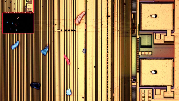
Visualizing Photoresist Residue and Organic Contamination on Wafers
As the scale of integrated circuits (ICs) on semiconductors passes below 10 nm, efficient detection of organic contamination, like photoresist residue, and defects during wafer inspection is becoming…
Loading...

Burr Detection During Battery Manufacturing
See how optical microscopy can be used for burr detection on battery electrodes and determination of damage potential to achieve rapid and reliable quality control during battery manufacturing.
Loading...

Battery Particle Detection During the Production Process
How battery particle detection and analysis is enhanced with optical microscopy and laser spectroscopy for rapid, reliable, and cost-effective QC during battery production is explained in this…
Loading...

Key Factors for Efficient Cleanliness Analysis
An overview of the key factors necessary for technical cleanliness and efficient cleanliness analysis concerning automotive and electronics manufacturing and production is provided in this article.
Loading...

Rapid Semiconductor Inspection with Microscope Contrast Methods
Semiconductor inspection during the production of patterned wafers and ICs (integrated circuits) is important for identifying and minimizing defects. To increase the efficiency of quality control in…
Loading...
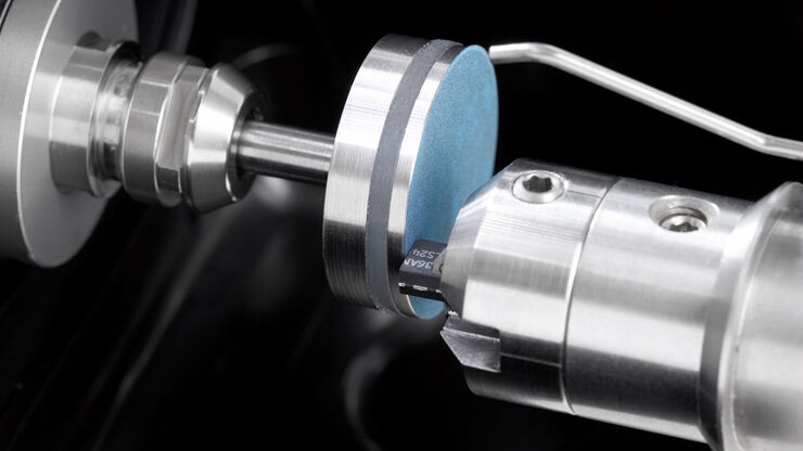
Cross-section Analysis for Electronics Manufacturing
This article describes cross-section analysis for electronics concerning quality control and failure analysis of printed circuit boards (PCBs) and assemblies (PCBAs), integrated circuits (ICs), etc.
Loading...
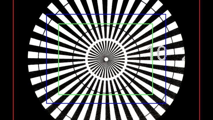
Understanding Clearly the Magnification of Microscopy
To help users better understand the magnification of microscopy and how to determine the useful range of magnification values for digital microscopes, this article provides helpful guidelines.
Loading...
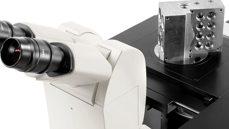
Five Inverted-Microscope Advantages for Industrial Applications
With inverted microscopes, you look at samples from below since their optics are placed under the sample, with upright microscopes you look at samples from above. Traditionally, inverted microscopes…
