Science Lab
Science Lab
Learn. Share. Contribute. The knowledge portal of Leica Microsystems. Find scientific research and teaching material on the subject of microscopy. The portal supports beginners, experienced practitioners and scientists alike in their everyday work and experiments. Explore interactive tutorials and application notes, discover the basics of microscopy as well as high-end technologies. Become part of the Science Lab community and share your expertise.
Filter articles
Tags
Story Type
Products
Loading...

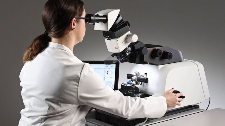
How to Save Time and Samples by Automated Ultramicrotomy
This article describes how 3D micro-CT data of a resin-embedded electron microscopy sample can be used to trim the specimen down to a defined target plane prior to sectioning. The interactive and…
Loading...

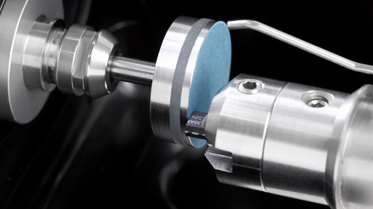
Essential Guide to Ultramicrotomy
When studying samples, to visualize their fine structure with nanometer scale resolution, most often electron microscopy is used. There are 2 types: scanning electron microscopy (SEM) which images the…
Loading...

The Guide to STED Sample Preparation
This guide is intended to help users optimize sample preparation for stimulated emission depletion (STED) nanoscopy, specifically when using the STED microscope from Leica Microsystems. It gives an…
Loading...

Cross-section Analysis for Electronics Manufacturing
This article describes cross-section analysis for electronics concerning quality control and failure analysis of printed circuit boards (PCBs) and assemblies (PCBAs), integrated circuits (ICs), etc.
Loading...

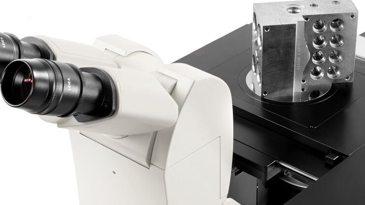
Five Inverted-Microscope Advantages for Industrial Applications
With inverted microscopes, you look at samples from below since their optics are placed under the sample, with upright microscopes you look at samples from above. Traditionally, inverted microscopes…
Loading...

High-Quality EBSD Sample Preparation
This article describes a method for EBSD sample preparation of challenging materials. The high-quality samples required for electron backscatter diffraction are prepared with broad ion-beam milling.
Loading...

How to Prepare and Analyse Battery Samples with Electron Microscopy
This workshop covers the sample preparation process for lithium and novel battery sample analysis, as well as other semiconductor samples requiring high-resolution cross-section imaging.
Loading...

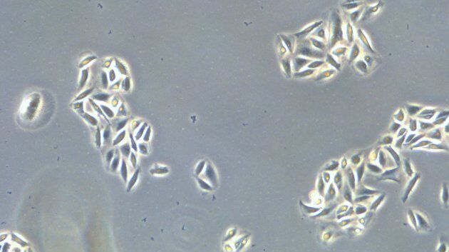
How to do a Proper Cell Culture Quick Check
In order to successfully work with mammalian cell lines, they must be grown under controlled conditions and require their own specific growth medium. In addition, to guarantee consistency their growth…
Loading...

RNA Quality after Different Tissue Sample Preparation
The influence of sample preparation and ultraviolet (UV) laser microdissection (UV LMD) on the quality of RNA from murine-brain tissue cryo-sections is described in this article. To obtain good…
