Electronics and Semiconductor Industry
For both electronics manufacturers and suppliers, efficient inspection, quality control (QC), failure analysis, and research & development (R&D), including cross-section and cleanliness analysis, are crucial. This goal applies to production of printed-circuit boards (PCBs) and assemblies (PCBAs), wafers, semiconductors, integrated-circuit (IC) chips, electroplated components, and battery systems, as well as product innovations. Solutions that help manufacturers and suppliers achieve cost-effective and reliable analysis of defects as well as preparation of component cross sections are advantageous. Cutting-edge technology and components for always better performing devices can be developed at competitive cost to stay ahead of the competition.
Please contact us if you would like to have personal expert advice on our microscopy solutions for electronics and semiconductor industry.
Select your field of application
What is the relationship between PCBs/PCBAs and electronics?
PCBs or PCBAs, printed circuit boards or assemblies, play a vital role in electronic devices like computers, smartphones, and electric vehicles. A PCBA is simply a PCB which has semiconductor components installed on it. PCBs and PCBAs undergo crucial inspection during production to ensure quality and reliability.
How are semiconductors used in electronics?
Semiconductor manufacturing creates components like integrated-circuit chips which are used on PCBs. These IC chips are made from layers of thin films deposited on a wafer composed of a semiconducting material like silicon. Inspection during semiconductor production is crucial for checking defects to ensure quality and reliability.
How are batteries used in electronics?
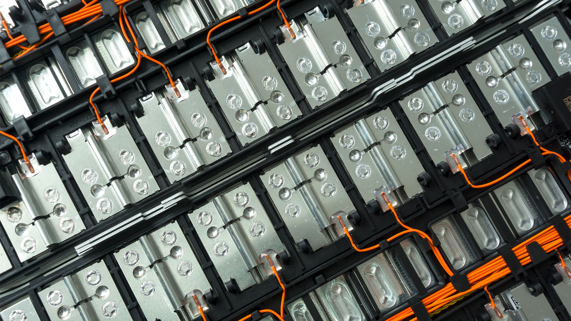
Batteries power a variety of devices, including smartphones, laptops, electric vehicles, power tools, and medical devices. They are crucial for applications in electronics, automobiles, and healthcare. Battery inspection involves checking for defects to ensure optimal performance and reliability.
PCBs – Fast and reliable QC
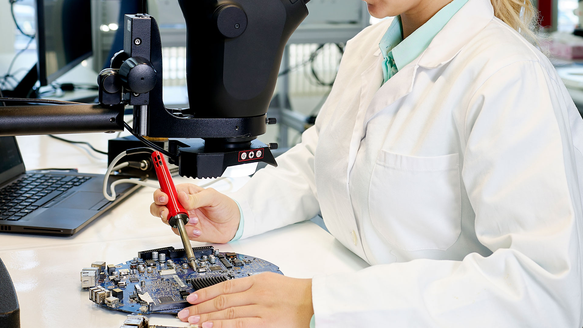
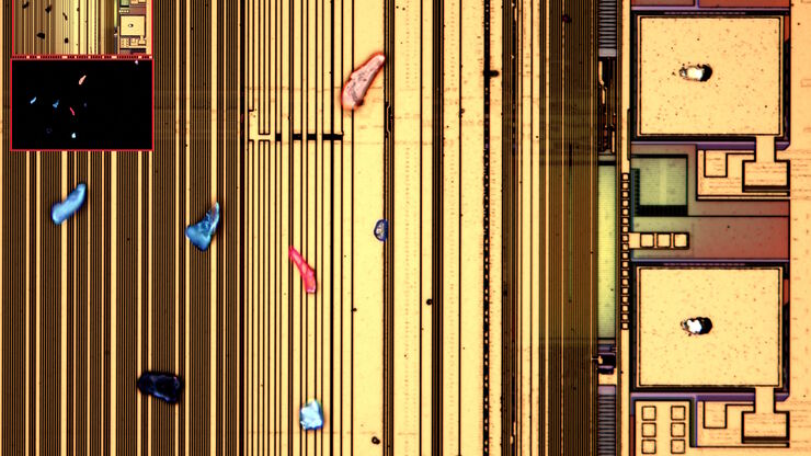
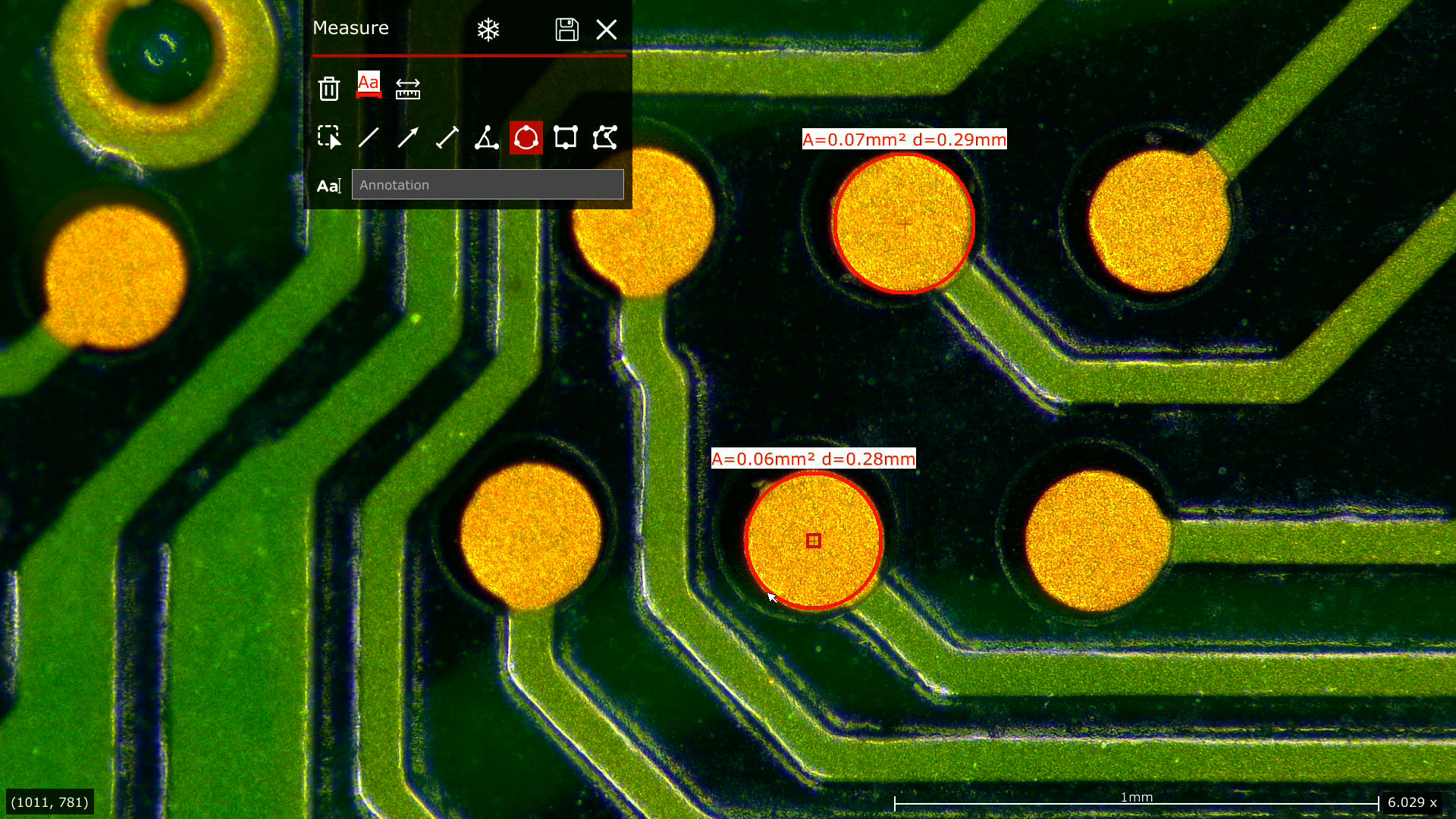
Quality control for PCBs and PCBAs can require inspection, rework, and cleanliness analysis. For electroplated components, the quality of the coating must be checked. PCB inspection should ensure proper soldering of IC chips and components and that there are no errors. Particulate contamination of PCBs during production must be kept under control to minimize the risk of poor performance or failure. Efficient and cost-effective QC of PCBs can be achieved with the right imaging solutions.
Find the microscope which fits best your needs for QC of PCBs:
Efficient inspection of semiconductors
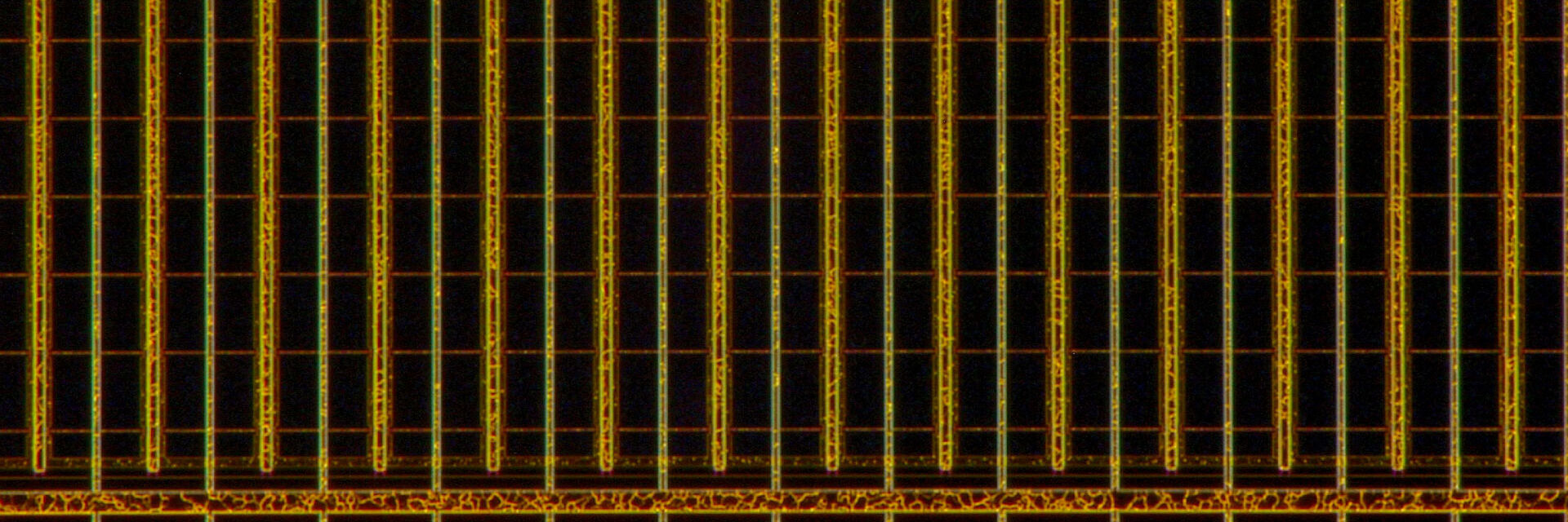
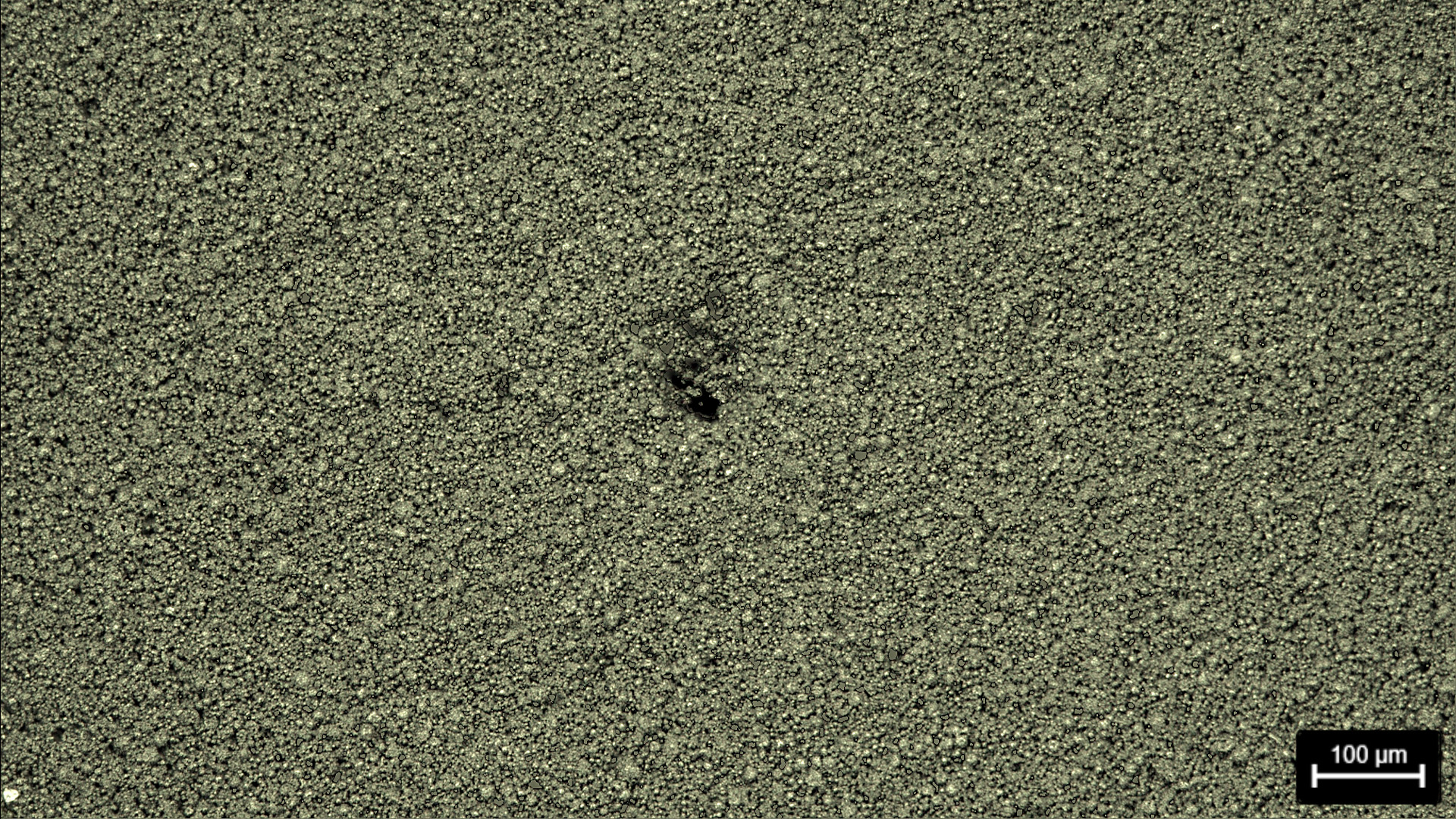
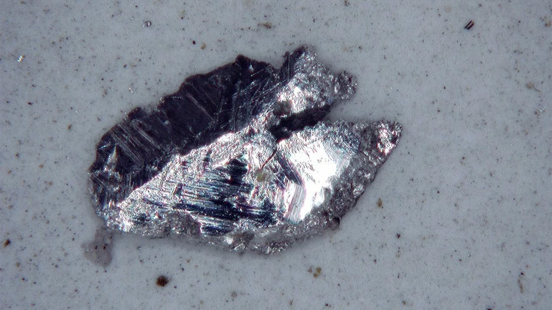
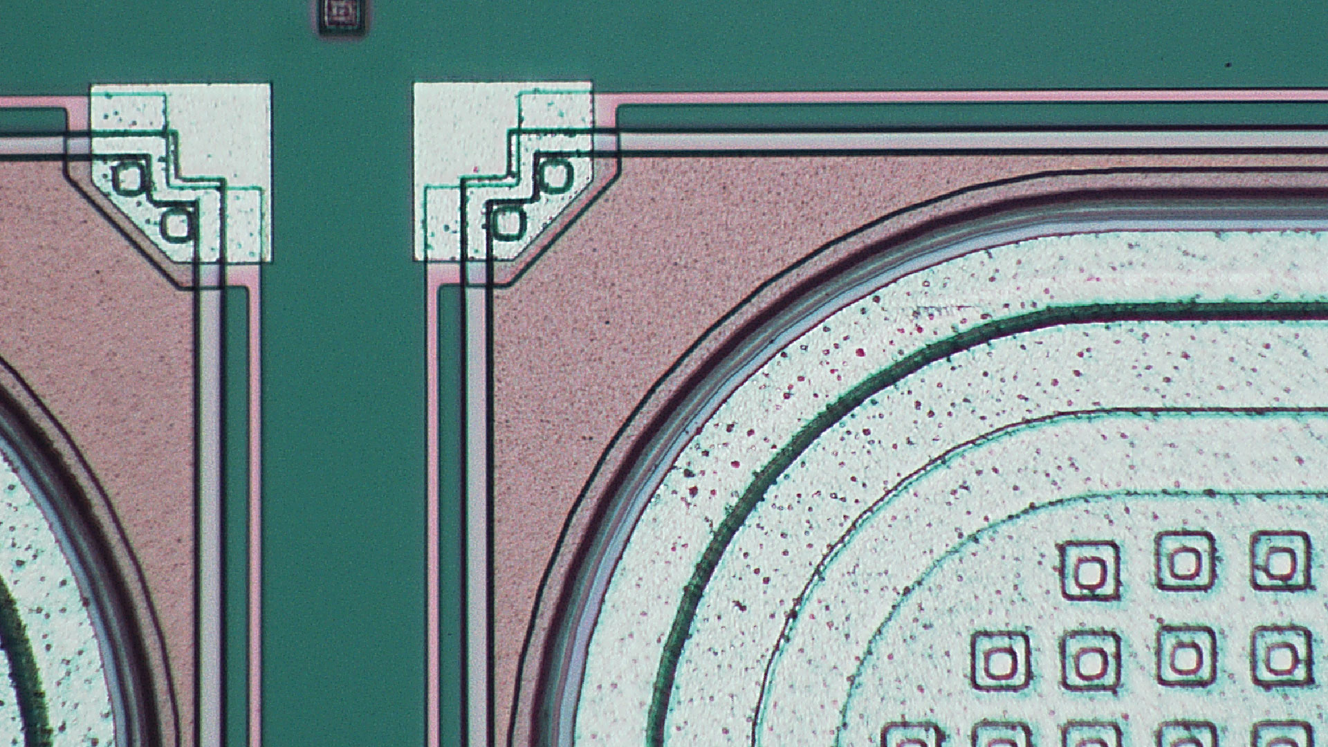
Inspection and analysis for wafers and IC chips during semiconductor device development and manufacturing must be fast, but also precise as it is essential to prove conformity to the target specifications. For IC-chip packaging and assembly, QC of electroplated leads is also mandatory.
Here you can understand the advantages of various microscopes in terms of your semiconductor QC and R&D requirements:
Battery manufacturing QC and development
Quality control for battery production necessitates efficient burr detection, electrode inspection, and cleanliness analysis for reliable battery performance, safe operation, and long lifetimes.
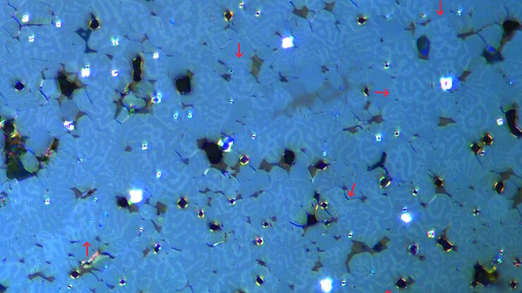
Burrs at electrode edges, critical defects on electrodes, and particle contamination can all cause short circuits and overheating. These problems often lead to poor battery performance or short lifetimes.
For batteries, burr detection, electrode inspection, and cleanliness analysis should be fast and reliable. The right microscope solutions can help.

Cross sectioning and analysis of electronic components
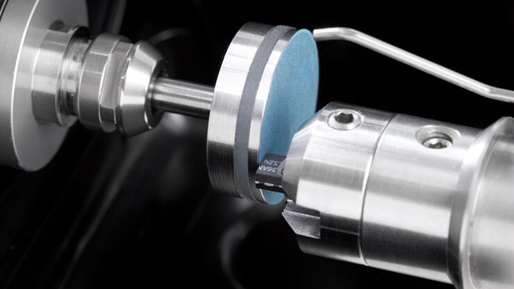
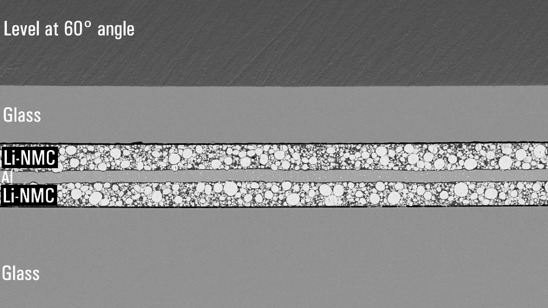
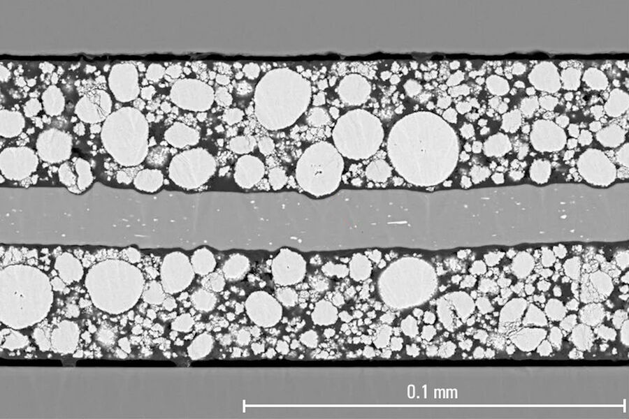
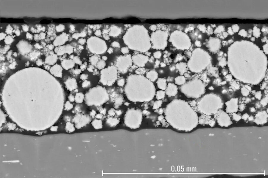
For QC, failure analysis, and R&D of PCBs, PCBAs, IC chips, and battery components, cross-section analysis is a practical way to examine their internal structure. As the materials are often opaque, the easiest way to access the internal structure is by making a cross section of the component. Then it can be analyzed visually and chemically with optical microscopy and spectroscopy or even electron microscopy and spectroscopy.
Discover more about solutions for rapid and reliable cross-section preparation as well as optical imaging and analysis:
Frequently asked questions Electronics and Semiconductor Industry
Semiconductors have an electrical conductivity between insulators (glass) and good conductors (metals). Intrinsic semiconductors, like pure silicon, have no impurities. Extrinsic semiconductors have impurities, like boron or phosphorus, called doping, which change their properties. Semiconductors are used to produce diodes and IC chips in computers, mobile devices, vehicles, medical equipment, etc.
Semiconductors have many properties which can be extremely useful for electronic devices. Components, IC chips, and devices made with semiconductors can rectify current, detect light and heat by converting them into electrical signals, amplify or switch on and off signals, emit light, etc.
The variable electrical properties of semiconductors are taken advantage of for electronics. Semiconductors which are doped have a conductivity between insulators and metals. These doped materials are used to make diodes, transistors, and IC chips to rectify currents, detect light and heat, amplify signals, emit light, etc.
Semiconductors are materials with an electrical conductivity between insulators and metals. Their properties make them useful for electronic components which rectify current, detect light and heat, amplify signals, emit light, etc.
Electronic components like diodes, transistors, amplifiers, integrated-circuit (IC) chips, sensors, CPUs, memory, and data storage devices are made with semiconductors. These components are used in computers, smart phones, tablets, automobiles, aircraft, ships, appliances, and medical equipment.
There are 2 basic types. Intrinsic semiconductors are pure, while extrinsic ones are doped, i.e., have impurities like boron (B) or phosphorus (P). A p-type semiconductor has extra "holes" or positive charges (absence of electrons), whereas an n-type has extra electrons.
Semiconductors are often made from silicon (Si), germanium (Ge), and gallium arsenide (GaAs). However, other materials are also possible.
Semiconductors are a critical part of many components used in almost every type of electronic device. Their variable properties make them very useful for making diodes, transistors, integrated-circuit (IC) chips, etc.
