DM8000 M & DM12000 M
Aufrechte Mikroskope
Lichtmikroskope
Produkte
Startseite
Leica Microsystems
DM8000 M & DM12000 M Optische Inspektionssysteme
Defekte schnell erkennen – bessere Entscheidungen treffen
Lesen Sie unsere neuesten Artikel

Visualizing Photoresist Residue and Organic Contamination on Wafers
As the scale of integrated circuits (ICs) on semiconductors passes below 10 nm, efficient detection of organic contamination, like photoresist residue, and defects during wafer inspection is becoming…
. Das Bild wurde mit einem Digitalmikroskop DVM6 aufgenommen.")
Graterkennung während der Batterieherstellung
Erfahren Sie, wie die optische Mikroskopie zur Graterkennung an Batterieelektroden und zur Bestimmung des Schadenspotenzials eingesetzt werden kann, um eine schnelle und zuverlässige…
 and oblique (right) brightfield illumination using a Leica compound microscope. The defect on the wafer surface is clearly more visible with oblique illumination.")
Rapid Semiconductor Inspection with Microscope Contrast Methods
Semiconductor inspection during the production of patterned wafers and ICs (integrated circuits) is important for identifying and minimizing defects. To increase the efficiency of quality control in…

How to Boost your Microelectronic Component Inspection Performance
Do you need to see more when inspecting silicon wafers or MEMS? Would you like to get sharp and detailed sample images which are similar to those from electron microscopes?
Watch this free webinar…
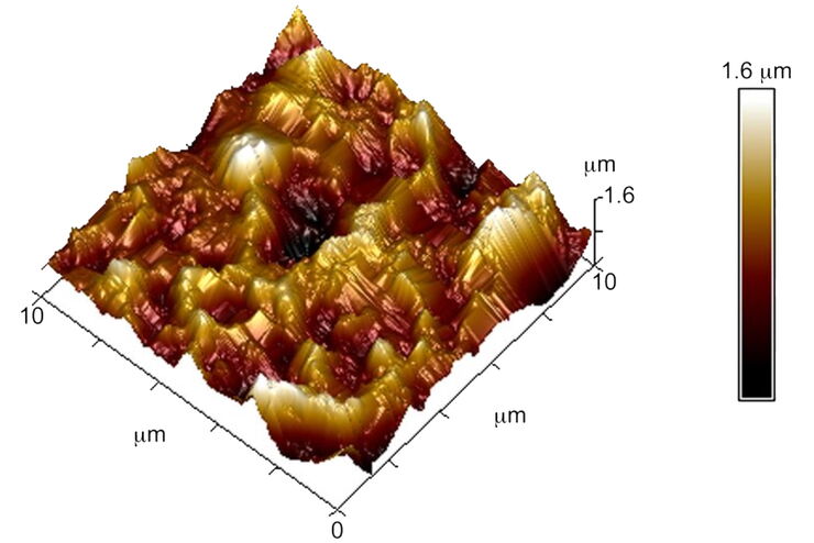
Brief Introduction to Surface Metrology
This report briefly discusses several important metrology techniques and standard definitions commonly used to assess the topography of surfaces, also known as surface texture or surface finish. With…
Fields of Application
Inspektionsmikroskope
Leica Microsystems bietet eine Vielzahl von Inspektionsmikroskopen für industrielle Anwendungen. Unsere Experten helfen Ihnen, die optimale Lösung zu finden.
Halbleiterinspektion
Erzielen Sie schnelle und zuverlässige Wafer- und Halbleiterprüfungen für die Waferverarbeitung sowie IC-Verpackung, -Montage und -Prüfung mit Mikroskop- und Probenvorbereitungslösungen.
