Biowissenschaften

Biowissenschaften

Biowissenschaften

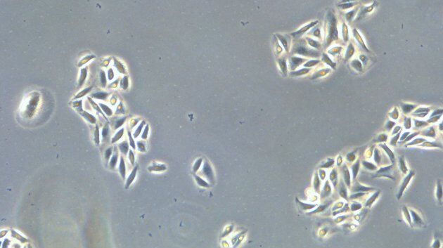
Hier können Sie Ihr Wissen, Ihre Forschungsfähigkeiten und Ihre praktischen Anwendungen der Mikroskopie in verschiedenen wissenschaftlichen Bereichen erweitern. Erfahren Sie, wie Sie präzise Visualisierung, Bildinterpretation und Forschungsfortschritte erzielen können. Hier finden Sie aufschlussreiche Informationen über fortgeschrittene Mikroskopie, Bildgebungsverfahren, Probenvorbereitung und Bildanalyse. Zu den behandelten Themen gehören Zellbiologie, Neurowissenschaften und Krebsforschung mit Schwerpunkt auf modernsten Anwendungen und Innovationen.
Optical microscope image, which is a composition of both brightfield and fluorescence illumination, showing organic contamination on a wafer surface. The inset images in the upper left corner show the brightfield image (above) and fluorescence image (below with dark background).

Visualizing Photoresist Residue and Organic Contamination on Wafers

As the scale of integrated circuits (ICs) on semiconductors passes below 10 nm, efficient detection of organic contamination, like photoresist residue, and defects during wafer inspection is becoming…
Eine Batterieelektrode, deren Ränder Grate aufweisen (mit roten Pfeilen markiert). Das Bild wurde mit einem Digitalmikroskop DVM6 aufgenommen.

Graterkennung während der Batterieherstellung

Erfahren Sie, wie die optische Mikroskopie zur Graterkennung an Batterieelektroden und zur Bestimmung des Schadenspotenzials eingesetzt werden kann, um eine schnelle und zuverlässige…
Images of the same area of a processed wafer taken with standard (left) and oblique (right) brightfield illumination using a Leica compound microscope. The defect on the wafer surface is clearly more visible with oblique illumination.

Rapid Semiconductor Inspection with Microscope Contrast Methods

Semiconductor inspection during the production of patterned wafers and ICs (integrated circuits) is important for identifying and minimizing defects. To increase the efficiency of quality control in…
Wafer

How to Boost your Microelectronic Component Inspection Performance

Do you need to see more when inspecting silicon wafers or MEMS? Would you like to get sharp and detailed sample images which are similar to those from electron microscopes? Watch this free webinar…

Brief Introduction to Surface Metrology

This report briefly discusses several important metrology techniques and standard definitions commonly used to assess the topography of surfaces, also known as surface texture or surface finish. With…
Scroll to top