DM8000 M y DM12000 M
Microscopios verticales
Microscopios ópticos
Productos
Inicio
Leica Microsystems
DM8000 M y DM12000 M Sistemas de inspección óptica
Detecte defectos rápidamente, tome mejores decisiones
Lea nuestros últimos artículos

Visualizing Photoresist Residue and Organic Contamination on Wafers
As the scale of integrated circuits (ICs) on semiconductors passes below 10 nm, efficient detection of organic contamination, like photoresist residue, and defects during wafer inspection is becoming…
 at the edge of a battery electrode acquired with a DVM6 digital microscope.")
Burr Detection During Battery Manufacturing
See how optical microscopy can be used for burr detection on battery electrodes and determination of damage potential to achieve rapid and reliable quality control during battery manufacturing.
 and oblique (right) brightfield illumination using a Leica compound microscope. The defect on the wafer surface is clearly more visible with oblique illumination.")
Rapid Semiconductor Inspection with Microscope Contrast Methods
Semiconductor inspection during the production of patterned wafers and ICs (integrated circuits) is important for identifying and minimizing defects. To increase the efficiency of quality control in…

How to Boost your Microelectronic Component Inspection Performance
Do you need to see more when inspecting silicon wafers or MEMS? Would you like to get sharp and detailed sample images which are similar to those from electron microscopes?
Watch this free webinar…
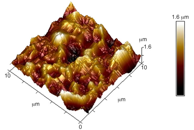
Brief Introduction to Surface Metrology
This report briefly discusses several important metrology techniques and standard definitions commonly used to assess the topography of surfaces, also known as surface texture or surface finish. With…
Campos de aplicación
Microscopios de inspección
Leica Microsystems ofrece una variedad de microscopios de inspección para aplicaciones industriales. Nuestros expertos pueden ayudarle a encontrar la solución óptima.
Inspección de semiconductores
Consiga una inspección rápida y fiable de obleas y semiconductores para el procesamiento de obleas, así como el empaquetado, el montaje y las pruebas de circuitos integrados, con soluciones de…
