
is mobile? false
Mercati della microscopia industriale
Negli ambienti industriali la tendenza attuale è di migliorare i tempi e raggiungere gli obiettivi in modo veloce per aumentare i profitti. Le soluzioni dedicate alle analisi microscopiche Leica, sono in grado di fornire informazioni sui più piccoli dettagli dei campioni e di analizzare, documentare e riportare i risultati in modo rapido e affidabile. Leica Microsystems offre un'ampia gamma di soluzioni e un'assistenza applicativa in grado di aiutarvi a soddisfare le vostre esigenze.
Leica Science Lab Show subnavigation
Leggi gli articoli più recenti
Il portale informativo di Leica Microsystems offre materiale didattico e di ricerca scientifica su vari temi della microscopia. Il contenuto è stato progettato per aiutare i principianti, i professionisti esperti e gli scienziati nel lavoro quotidiano e negli esperimenti.

Automotive Part Verification and Development according to Specifications
Automotive part verification during the development and production of parts and components by suppliers or manufacturers is important for ensuring that specifications are met. Specifications are critical for maintaining performance standards and safe operation of vehicles. However, there is always demand for efficient and cost-effective R&D and production while meeting ever-stricter quality standards. This article shows how investigation and documentation of auto parts and components to verify specifications can be done easily and quickly with digital microscopy.

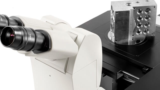
Microscopi per campo scuro
Il metodo di contrasto in campo oscuro sfrutta la diffrazione o la dispersione della luce da strutture di un campione biologico o da caratteristiche non uniformi nella struttura di un materiale.

The Polarization Microscopy Principle
Polarization microscopy is routinely used in the material and earth sciences to identify materials and minerals on the basis of their characteristic refractive properties and colors. In biology, polarization microscopes are commonly used for identification of birefringent structures, like crystals, or for imaging of cellulose in the walls of plant cells and starch grains. This article gives an overview of the basic principles of polarization microscopy.

Rapidly Visualizing Magnetic Domains in Steel with Kerr Microscopy
The rotation of polarized light after interaction with magnetic domains in a material, known as the Kerr effect, enables the investigation of magnetized samples with Kerr microscopy. It allows rapid visualization of magnetic domains at the material’s surface. For efficient R&D and QC of magnetic materials, e.g., steel alloys, used in electrical and electronic devices, Kerr microscopy can play an important role. More details about how Kerr microscopy can be used to image magnetic domains in the grains of steel alloys is described in this article.

6-Inch Wafer Inspection Microscope for Reliably Observing Small Height Differences
A 6-inch wafer inspection microscope with automated and reproducible DIC (differential interference contrast) imaging, no matter the skill level of users, is described in this article. Manufacturing of integrated-circuit (IC) chips and semiconductor components requires wafer inspection to verify no defects are present which affect performance. The inspection is often done with optical microscopy for QC, failure analysis, and R&D. To visualize efficiently small height differences between structures on wafers, DIC can be used.

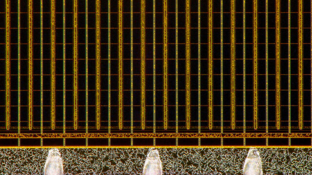
Visualizing Photoresist Residue and Organic Contamination on Wafers
As the scale of integrated circuits (ICs) on semiconductors passes below 10 nm, efficient detection of organic contamination, like photoresist residue, and defects during wafer inspection is becoming more crucial. Optical microscopy is still the common inspection method, but for organic contamination brightfield and other types of illumination can have limitations. How fluorescence microscopy is used to efficiently detect photoresist residues and other organic contamination on wafers during QC, failure analysis, and R&D for the semiconductor industry is discussed in this article.

Workflow Solutions for Sample Preparation Methods for Material Science
This brochure presents and explains appropriate workflow solutions for the most frequently required sample preparation methods for material science samples.

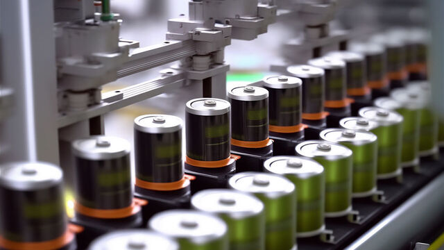
Burr Detection During Battery Manufacturing
See how optical microscopy can be used for burr detection on battery electrodes and determination of damage potential to achieve rapid and reliable quality control during battery manufacturing.

Battery Particle Detection During the Production Process
How battery particle detection and analysis is enhanced with optical microscopy and laser spectroscopy for rapid, reliable, and cost-effective QC during battery production is explained in this article.

Key Factors for Efficient Cleanliness Analysis
An overview of the key factors necessary for technical cleanliness and efficient cleanliness analysis concerning automotive and electronics manufacturing and production is provided in this article.

Technical Terms for Digital Microscope Cameras and Image Analysis
Learn more about the basic principles behind digital microscope camera technologies, how digital cameras work, and take advantage of a reference list of technical terms from this article.

Rapid Semiconductor Inspection with Microscope Contrast Methods
Semiconductor inspection during the production of patterned wafers and ICs (integrated circuits) is important for identifying and minimizing defects. To increase the efficiency of quality control in the early stages of production and to ensure reliable IC chip performance, microscopy solutions should combine different contrast methods that provide complete and accurate information about different defects. Our free guide details microscopy techniques & optimizing quality control. Get your free copy today!

Cross-section Analysis for Electronics Manufacturing
This article describes cross-section analysis for electronics concerning quality control and failure analysis of printed circuit boards (PCBs) and assemblies (PCBAs), integrated circuits (ICs), etc.

Understanding Clearly the Magnification of Microscopy
To help users better understand the magnification of microscopy and how to determine the useful range of magnification values for digital microscopes, this article provides helpful guidelines.

Five Inverted-Microscope Advantages for Industrial Applications
With inverted microscopes, you look at samples from below since their optics are placed under the sample, with upright microscopes you look at samples from above. Traditionally, inverted microscopes are used for life science research, because gravity makes samples sink to the bottom of a holder with aqueous solution and you don’t see a lot from above.

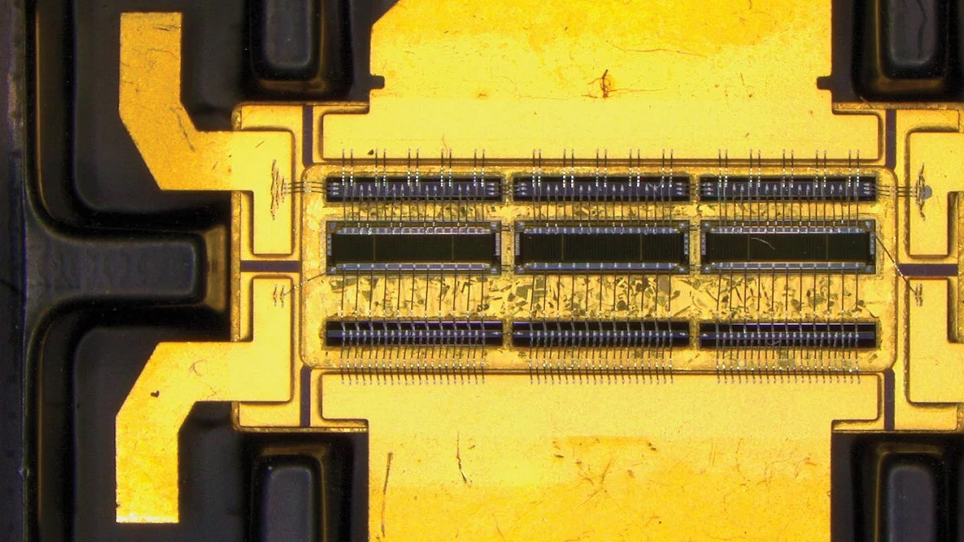
Structural and Chemical Analysis of IC-Chip Cross Sections
This article shows how electronic IC-chip cross sections can be efficiently and reliably prepared and then analyzed, both visually and chemically at the microscale, with the EM TXP and DM6 M LIBS solutions.