
Filter articles
标签
Products
Loading...

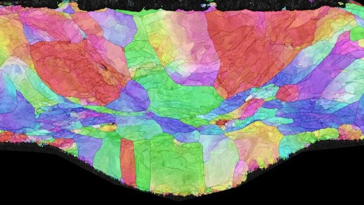
The Polarization Microscopy Principle
Polarization microscopy is routinely used in the material and earth sciences to identify materials and minerals on the basis of their characteristic refractive properties and colors. In biology,…
Loading...
. With DIC users are able to visualize small height differences on the wafer surface more easily.")
6-Inch Wafer Inspection Microscope for Reliably Observing Small Height Differences
A 6-inch wafer inspection microscope with automated and reproducible DIC (differential interference contrast) imaging, no matter the skill level of users, is described in this article. Manufacturing…
Loading...
Workflow Solutions for Sample Preparation Methods for Material Science
This brochure presents and explains appropriate workflow solutions for the most frequently required sample preparation methods for material science samples.
Loading...

Key Factors for Efficient Cleanliness Analysis
An overview of the key factors necessary for technical cleanliness and efficient cleanliness analysis concerning automotive and electronics manufacturing and production is provided in this article.
Loading...
 and oblique (right) brightfield illumination using a Leica compound microscope. The defect on the wafer surface is clearly more visible with oblique illumination.")
Rapid Semiconductor Inspection with Microscope Contrast Methods
Semiconductor inspection during the production of patterned wafers and ICs (integrated circuits) is important for identifying and minimizing defects. To increase the efficiency of quality control in…
Loading...

Cross-section Analysis for Electronics Manufacturing
This article describes cross-section analysis for electronics concerning quality control and failure analysis of printed circuit boards (PCBs) and assemblies (PCBAs), integrated circuits (ICs), etc.
Loading...

Five Inverted-Microscope Advantages for Industrial Applications
With inverted microscopes, you look at samples from below since their optics are placed under the sample, with upright microscopes you look at samples from above. Traditionally, inverted microscopes…
Loading...

Rapid and Reliable Examination of PCBs & PCBAs with Digital Microscopy
Digital microscopes provide users with a convenient and rapid way to acquire high-quality, reliable image data and make quick inspection and analysis of printed circuit boards (PCBs) and assemblies…
Loading...

What is the FusionOptics Technology?
Leica stereo microscopes with FusionOptics provide optimal 3D perception. The brain merges two images, one with large depth of field and the other with high resolution, into one 3D image.
