
Filter articles
标签
Story Type
Products
Loading...

Automotive Part Verification and Development according to Specifications
Automotive part verification during the development and production of parts and components by suppliers or manufacturers is important for ensuring that specifications are met. Specifications are…
Loading...

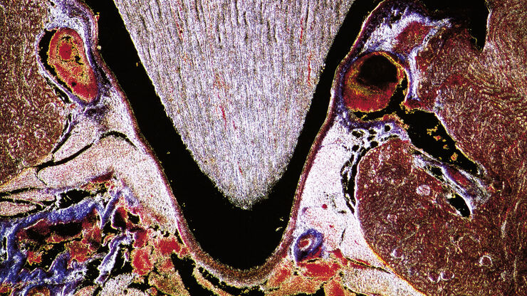
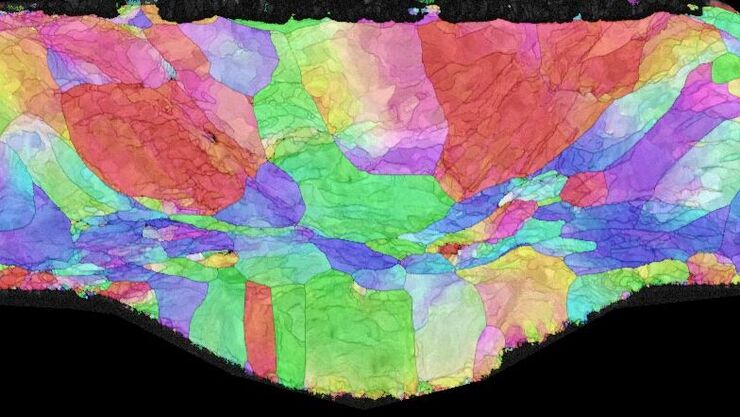
The Polarization Microscopy Principle
Polarization microscopy is routinely used in the material and earth sciences to identify materials and minerals on the basis of their characteristic refractive properties and colors. In biology,…
Loading...

Rapidly Visualizing Magnetic Domains in Steel with Kerr Microscopy
The rotation of polarized light after interaction with magnetic domains in a material, known as the Kerr effect, enables the investigation of magnetized samples with Kerr microscopy. It allows rapid…
Loading...
. With DIC users are able to visualize small height differences on the wafer surface more easily.")
6-Inch Wafer Inspection Microscope for Reliably Observing Small Height Differences
A 6-inch wafer inspection microscope with automated and reproducible DIC (differential interference contrast) imaging, no matter the skill level of users, is described in this article. Manufacturing…
Loading...

Visualizing Photoresist Residue and Organic Contamination on Wafers
As the scale of integrated circuits (ICs) on semiconductors passes below 10 nm, efficient detection of organic contamination, like photoresist residue, and defects during wafer inspection is becoming…
Loading...
Workflow Solutions for Sample Preparation Methods for Material Science
This brochure presents and explains appropriate workflow solutions for the most frequently required sample preparation methods for material science samples.
Loading...
 at the edge of a battery electrode acquired with a DVM6 digital microscope.")
Burr Detection During Battery Manufacturing
See how optical microscopy can be used for burr detection on battery electrodes and determination of damage potential to achieve rapid and reliable quality control during battery manufacturing.
Loading...

Battery Particle Detection During the Production Process
How battery particle detection and analysis is enhanced with optical microscopy and laser spectroscopy for rapid, reliable, and cost-effective QC during battery production is explained in this…
